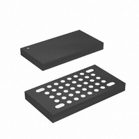
ATMEGA16HVA-4CKU Atmel, ATMEGA16HVA-4CKU Datasheet - Page 70

ATMEGA16HVA-4CKU
Manufacturer Part Number
ATMEGA16HVA-4CKU
Description
MCU AVR 16K FLASH 4MHZ 36-LGA
Manufacturer
Atmel
Series
AVR® ATmegar
Datasheet
1.ATMEGA16HVA-4CKU.pdf
(196 pages)
Specifications of ATMEGA16HVA-4CKU
Core Processor
AVR
Core Size
8-Bit
Speed
4MHz
Connectivity
SPI
Peripherals
Brown-out Detect/Reset, POR, PWM, WDT
Number Of I /o
7
Program Memory Size
16KB (8K x 16)
Program Memory Type
FLASH
Eeprom Size
256 x 8
Ram Size
512 x 8
Voltage - Supply (vcc/vdd)
1.8 V ~ 9 V
Data Converters
A/D 5x12b
Oscillator Type
External
Operating Temperature
-20°C ~ 85°C
Package / Case
36-LGA
Processor Series
ATMEGA16x
Core
AVR8
Data Bus Width
8 bit
Data Ram Size
512 B
Interface Type
SPI
Maximum Clock Frequency
4 MHz
Number Of Programmable I/os
6
Number Of Timers
2
Maximum Operating Temperature
+ 85 C
Mounting Style
SMD/SMT
3rd Party Development Tools
EWAVR, EWAVR-BL
Development Tools By Supplier
ATAVRDRAGON, ATSTK500, ATSTK600, ATAVRISP2, ATAVRONEKIT, ATAVRSB200, ATAVRSB201
Minimum Operating Temperature
- 20 C
On-chip Adc
12 bit, 5 Channel
For Use With
ATSTK600 - DEV KIT FOR AVR/AVR32ATSTK500 - PROGRAMMER AVR STARTER KIT
Lead Free Status / RoHS Status
Lead free / RoHS Compliant
- Current page: 70 of 196
- Download datasheet (3Mb)
15.3.1
70
ATmega8HVA/16HVA
Alternate Functions of Port A
The Port A pins with alternate functions are shown in
Table 15-3.
The alternate pin configuration is as follows:
• ADC0/ SNGD/ T0 – Port A, Bit 0
Voltage Analog to Digital Converter (Channel 0), Signal Ground for Voltage Analog to Digital
Converter or Timer/Counter0 Counter Source.
• ADC1/ SNGD/ T1 – Port A, Bit 1
Voltage Analog to Digital Converter (Channel 1) , Signal Ground for Voltage Analog to Digital
Converter or Timer/Counter1 Counter Source.
Table 15-4
5 on page
Table 15-4.
Signal Name
PUOE
PUOV
DDOE
DDOV
PVOE
PVOV
PTOE
DIEOE
DIEOV
DI
AIO
Port Pin
68.
relates the alternate functions of Port A to the overriding signals shown in
PA1
PA0
Port A Pins Alternate Functions
Overriding Signals for Alternate Functions in PA1..PA0
PA0/ADC0/SGND/T0
0
0
0
0
0
0
–
PA0DID
0
–
ADC0 INPUT/ SGND/ T0
Alternate Function
ADC1/ SGND/ T1 (ADC Input Channel 1, Signal Ground or
Timer/Counter1 Clock Input)
ADC0/ SGND/ T0 (ADC Input Channel 0, Signal Ground or
Timer/Counter0 Clock Input))
Table
PA1/ADC1/SGND/T1
0
0
0
0
0
0
–
PA1DID
0
–
ADC1 INPUT/ SGND/ T1
15-3.
8024A–AVR–04/08
Figure 15-
Related parts for ATMEGA16HVA-4CKU
Image
Part Number
Description
Manufacturer
Datasheet
Request
R

Part Number:
Description:
DEV KIT FOR AVR/AVR32
Manufacturer:
Atmel
Datasheet:

Part Number:
Description:
INTERVAL AND WIPE/WASH WIPER CONTROL IC WITH DELAY
Manufacturer:
ATMEL Corporation
Datasheet:

Part Number:
Description:
Low-Voltage Voice-Switched IC for Hands-Free Operation
Manufacturer:
ATMEL Corporation
Datasheet:

Part Number:
Description:
MONOLITHIC INTEGRATED FEATUREPHONE CIRCUIT
Manufacturer:
ATMEL Corporation
Datasheet:

Part Number:
Description:
AM-FM Receiver IC U4255BM-M
Manufacturer:
ATMEL Corporation
Datasheet:

Part Number:
Description:
Monolithic Integrated Feature Phone Circuit
Manufacturer:
ATMEL Corporation
Datasheet:

Part Number:
Description:
Multistandard Video-IF and Quasi Parallel Sound Processing
Manufacturer:
ATMEL Corporation
Datasheet:

Part Number:
Description:
High-performance EE PLD
Manufacturer:
ATMEL Corporation
Datasheet:

Part Number:
Description:
8-bit Flash Microcontroller
Manufacturer:
ATMEL Corporation
Datasheet:

Part Number:
Description:
2-Wire Serial EEPROM
Manufacturer:
ATMEL Corporation
Datasheet:


