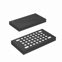
ATMEGA16HVA-4CKU Atmel, ATMEGA16HVA-4CKU Datasheet - Page 115

ATMEGA16HVA-4CKU
Manufacturer Part Number
ATMEGA16HVA-4CKU
Description
MCU AVR 16K FLASH 4MHZ 36-LGA
Manufacturer
Atmel
Series
AVR® ATmegar
Datasheet
1.ATMEGA16HVA-4CKU.pdf
(196 pages)
Specifications of ATMEGA16HVA-4CKU
Core Processor
AVR
Core Size
8-Bit
Speed
4MHz
Connectivity
SPI
Peripherals
Brown-out Detect/Reset, POR, PWM, WDT
Number Of I /o
7
Program Memory Size
16KB (8K x 16)
Program Memory Type
FLASH
Eeprom Size
256 x 8
Ram Size
512 x 8
Voltage - Supply (vcc/vdd)
1.8 V ~ 9 V
Data Converters
A/D 5x12b
Oscillator Type
External
Operating Temperature
-20°C ~ 85°C
Package / Case
36-LGA
Processor Series
ATMEGA16x
Core
AVR8
Data Bus Width
8 bit
Data Ram Size
512 B
Interface Type
SPI
Maximum Clock Frequency
4 MHz
Number Of Programmable I/os
6
Number Of Timers
2
Maximum Operating Temperature
+ 85 C
Mounting Style
SMD/SMT
3rd Party Development Tools
EWAVR, EWAVR-BL
Development Tools By Supplier
ATAVRDRAGON, ATSTK500, ATSTK600, ATAVRISP2, ATAVRONEKIT, ATAVRSB200, ATAVRSB201
Minimum Operating Temperature
- 20 C
On-chip Adc
12 bit, 5 Channel
For Use With
ATSTK600 - DEV KIT FOR AVR/AVR32ATSTK500 - PROGRAMMER AVR STARTER KIT
Lead Free Status / RoHS Status
Lead free / RoHS Compliant
- Current page: 115 of 196
- Download datasheet (3Mb)
20.4.3
8024A–AVR–04/08
VADCL and VADCH – V-ADC Data Register
VADSC will read as one as long as the conversion is not finished. When the conversion is com-
plete, it returns to zero. Writing zero to this bit has no effect. VADSC will automatically be
cleared when the VADEN bit is written to zero.
• Bit 1 – VADCCIF: V-ADC Conversion Complete Interrupt Flag
This bit is set when a V-ADC conversion completes and the data registers are updated. The V-
ADC Conversion Complete Interrupt is executed if the VADCCIE bit and the I-bit in SREG are
set. VADCCIF is cleared by hardware when executing the corresponding interrupt handling vec-
tor. Alternatively, VADCCIF is cleared by writing a logical one to the flag. Beware that if doing a
Read-Modify-Write on VADCSR, a pending interrupt can be lost.
• Bit 0 – VADCCIE: V-ADC Conversion Complete Interrupt Enable
When this bit is written to one and the I-bit in SREG is set, the V-ADC Conversion Complete
Interrupt is activated.
When a V-ADC conversion is complete, the result is found in these two registers. To ensure that
correct data is read, both high and low byte data registers should be read before starting a new
conversion.
• VADC11:0: V-ADC Conversion Result
These bits represent the result from the conversion.
To obtain the best absolute accuracy for the cell voltage measurements, gain and offset com-
pensation is required. Factory calibration values are stored in the device signature row, refer to
section "Reading the Signature Row from Software" on page 144 for details. The cell voltage in
mV is given by:
The voltage on the ADCn is given by:
When performing a VTEMP conversion, the result must be adjusted by the factory calibration
value stored in the signature row, refer to section
on page 144
Bit
(0x79)
(0x78)
Read/Write
Initial Value
ADCn[mV]
Cell
for details. The absolute temperature in Kelvin is given by:
n
[mV]
15
R
R
–
7
0
0
=
----- - (VADCH/L VADC ADCn Offset)
10
1
=
⋅
(VADCH/L VADC Cell
------------------------------------------------------------------------------------------------------------------------------------------------------------------------------------- -
----------------------------------------------------------------------------------------------------------------------------------------------------------------------------------------------
14
R
R
–
6
0
0
–
–
13
R
R
–
5
0
0
12
n
R
R
–
4
0
0
Offset)
VADC[7:0]
16384
”Reading the Signature Row from Software”
⋅
11
16384
VADC Cell
3
R
R
0
0
⋅
ATmega8HVA/16HVA
VADC ADCn Gain Calibration Word
10
R
R
0
2
0
n
VADC[11:8]
Gain Calibration Word
R
R
9
1
0
0
R
R
8
0
0
0
VADCH
VADCL
115
Related parts for ATMEGA16HVA-4CKU
Image
Part Number
Description
Manufacturer
Datasheet
Request
R

Part Number:
Description:
DEV KIT FOR AVR/AVR32
Manufacturer:
Atmel
Datasheet:

Part Number:
Description:
INTERVAL AND WIPE/WASH WIPER CONTROL IC WITH DELAY
Manufacturer:
ATMEL Corporation
Datasheet:

Part Number:
Description:
Low-Voltage Voice-Switched IC for Hands-Free Operation
Manufacturer:
ATMEL Corporation
Datasheet:

Part Number:
Description:
MONOLITHIC INTEGRATED FEATUREPHONE CIRCUIT
Manufacturer:
ATMEL Corporation
Datasheet:

Part Number:
Description:
AM-FM Receiver IC U4255BM-M
Manufacturer:
ATMEL Corporation
Datasheet:

Part Number:
Description:
Monolithic Integrated Feature Phone Circuit
Manufacturer:
ATMEL Corporation
Datasheet:

Part Number:
Description:
Multistandard Video-IF and Quasi Parallel Sound Processing
Manufacturer:
ATMEL Corporation
Datasheet:

Part Number:
Description:
High-performance EE PLD
Manufacturer:
ATMEL Corporation
Datasheet:

Part Number:
Description:
8-bit Flash Microcontroller
Manufacturer:
ATMEL Corporation
Datasheet:

Part Number:
Description:
2-Wire Serial EEPROM
Manufacturer:
ATMEL Corporation
Datasheet:


