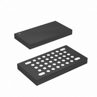
ATMEGA16HVA-4CKU Atmel, ATMEGA16HVA-4CKU Datasheet - Page 136

ATMEGA16HVA-4CKU
Manufacturer Part Number
ATMEGA16HVA-4CKU
Description
MCU AVR 16K FLASH 4MHZ 36-LGA
Manufacturer
Atmel
Series
AVR® ATmegar
Datasheet
1.ATMEGA16HVA-4CKU.pdf
(196 pages)
Specifications of ATMEGA16HVA-4CKU
Core Processor
AVR
Core Size
8-Bit
Speed
4MHz
Connectivity
SPI
Peripherals
Brown-out Detect/Reset, POR, PWM, WDT
Number Of I /o
7
Program Memory Size
16KB (8K x 16)
Program Memory Type
FLASH
Eeprom Size
256 x 8
Ram Size
512 x 8
Voltage - Supply (vcc/vdd)
1.8 V ~ 9 V
Data Converters
A/D 5x12b
Oscillator Type
External
Operating Temperature
-20°C ~ 85°C
Package / Case
36-LGA
Processor Series
ATMEGA16x
Core
AVR8
Data Bus Width
8 bit
Data Ram Size
512 B
Interface Type
SPI
Maximum Clock Frequency
4 MHz
Number Of Programmable I/os
6
Number Of Timers
2
Maximum Operating Temperature
+ 85 C
Mounting Style
SMD/SMT
3rd Party Development Tools
EWAVR, EWAVR-BL
Development Tools By Supplier
ATAVRDRAGON, ATSTK500, ATSTK600, ATAVRISP2, ATAVRONEKIT, ATAVRSB200, ATAVRSB201
Minimum Operating Temperature
- 20 C
On-chip Adc
12 bit, 5 Channel
For Use With
ATSTK600 - DEV KIT FOR AVR/AVR32ATSTK500 - PROGRAMMER AVR STARTER KIT
Lead Free Status / RoHS Status
Lead free / RoHS Compliant
- Current page: 136 of 196
- Download datasheet (3Mb)
24.2
24.2.1
24.2.2
136
FET Driver
ATmega8HVA/16HVA
Features
Overview
•
•
The ATmega8HVA/16HVA includes a FET Driver. The FET Driver is designed for driving N-
channel FETs used as high side switch in 1- or 2-Cell Li-Ion battery pack. A block diagram of the
FET driver is shown in
When charging deeply over-discharged cells, the FET Driver will be operated in Deep Under-
Voltage Recovery (DUVR) mode. In DUVR mode the FET Driver regulates the voltage at the
VFET pin to typically 2.0 Volts in 1-Cell applications and typically 4.0 Volts in 2-Cell applications.
This is done by operating the Charge FET at a point where the drain-source voltage is equal to
the voltage difference between the cell voltage and the required VFET operating voltage. As the
cell voltage increases, the drain-source voltage of the Charge FET will decrease until the
Charge FET is completely on. See
In normal operation (DUVRD = 1), the Charge FET/Discharge FET is switched on by pumping
OC/OD sufficiently above the VFET supply voltage. To turn off the Charge FET/Discharge FET,
OC/OD is pulled quickly low. See
details.
Figure 24-2. FET Driver block diagram.
Charge-pump for generating suitable gate drive for N-Channel FET switch on high side
Deep Under-voltage Recovery mode that allows normal operation while charging a Deeply Over-
discharged battery from 0-volt
BANDGAP
CONTROL
_VREG
LDO
REF.
FET
CLK
Figure 24-2 on page
DUVRD
CHARGE_EN
DISCHARGE_EN
CLK_OSC
DVDD
DUALC_MODE
VREF
Table 29-5 on page 170
Figure 24-3 on page 137
Charge
C-FET
Pump
14V clamp
136.
Charge FET
Charge
D-FET
1k
Pump
NFET DRIVER
Discharge FET
1k
for details.
14V clamp
and
Table 29-5 on page 170
BATT+
BATT-
8024A–AVR–04/08
for
Related parts for ATMEGA16HVA-4CKU
Image
Part Number
Description
Manufacturer
Datasheet
Request
R

Part Number:
Description:
DEV KIT FOR AVR/AVR32
Manufacturer:
Atmel
Datasheet:

Part Number:
Description:
INTERVAL AND WIPE/WASH WIPER CONTROL IC WITH DELAY
Manufacturer:
ATMEL Corporation
Datasheet:

Part Number:
Description:
Low-Voltage Voice-Switched IC for Hands-Free Operation
Manufacturer:
ATMEL Corporation
Datasheet:

Part Number:
Description:
MONOLITHIC INTEGRATED FEATUREPHONE CIRCUIT
Manufacturer:
ATMEL Corporation
Datasheet:

Part Number:
Description:
AM-FM Receiver IC U4255BM-M
Manufacturer:
ATMEL Corporation
Datasheet:

Part Number:
Description:
Monolithic Integrated Feature Phone Circuit
Manufacturer:
ATMEL Corporation
Datasheet:

Part Number:
Description:
Multistandard Video-IF and Quasi Parallel Sound Processing
Manufacturer:
ATMEL Corporation
Datasheet:

Part Number:
Description:
High-performance EE PLD
Manufacturer:
ATMEL Corporation
Datasheet:

Part Number:
Description:
8-bit Flash Microcontroller
Manufacturer:
ATMEL Corporation
Datasheet:

Part Number:
Description:
2-Wire Serial EEPROM
Manufacturer:
ATMEL Corporation
Datasheet:


