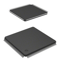
HD6417706F133 Renesas Electronics America, HD6417706F133 Datasheet - Page 103

HD6417706F133
Manufacturer Part Number
HD6417706F133
Description
IC SUPERH MPU ROMLESS 176LQFP
Manufacturer
Renesas Electronics America
Series
SuperH® SH7700r
Datasheet
1.HD6417706F133V.pdf
(751 pages)
Specifications of HD6417706F133
Core Processor
SH-3
Core Size
32-Bit
Speed
133MHz
Connectivity
EBI/EMI, FIFO, SCI, SmartCard
Peripherals
DMA, POR, WDT
Number Of I /o
103
Program Memory Type
ROMless
Ram Size
16K x 8
Voltage - Supply (vcc/vdd)
1.75 V ~ 2.05 V
Oscillator Type
Internal
Operating Temperature
-20°C ~ 75°C
Package / Case
176-LQFP
Lead Free Status / RoHS Status
Contains lead / RoHS non-compliant
Eeprom Size
-
Program Memory Size
-
Data Converters
-
Available stocks
Company
Part Number
Manufacturer
Quantity
Price
Part Number:
HD6417706F133
Manufacturer:
RENESAS/瑞萨
Quantity:
20 000
Company:
Part Number:
HD6417706F133V
Manufacturer:
EDISON
Quantity:
2 000
Company:
Part Number:
HD6417706F133V
Manufacturer:
Renesas Electronics America
Quantity:
10 000
Part Number:
HD6417706F133V
Manufacturer:
RENESAS/瑞萨
Quantity:
20 000
- Current page: 103 of 751
- Download datasheet (5Mb)
Section 3 Memory Management Unit (MMU)
3.1.1
This LSI's MMU
Virtual Address Map: This LSI uses 32-bit virtual addresses to access a 4-Gbyte virtual address
space that is divided into several areas. Address space mapping is shown in figure 3.2.
In the privileged mode, the virtual address space is divided into five areas.
P0 and P3 areas are mapped to physical address spaces in page units according to the information
in the address translation table. Write-back or write-through can be selected for write access by
means of a cache control register (CCR) setting.
Mapping of the P1 area is fixed to physical address space (H'00000000 to H'1FFFFFFF). In the P1
area, setting a virtual address MSBs (bit 31) to 0 generates the corresponding physical address. P1
area access can be cached, write-back or write-through can be selected according to the setting of
CCR whether to cache or not.
Mapping of the P2 area is fixed to physical address space (H'00000000 to H'1FFFFFFF). In the P2
area, setting the top three virtual address bits (bits 31, 30, and 29) to 0 generates the corresponding
physical address. P2 area access cannot be cached.
The P1 and P2 areas are not mapped by the address translation table, so the TLB is not used and
no exceptions like TLB misses occur. Initialization of MMU-related registers, exception
processing, and the like are located in the P1 and P2 areas. Because the P1 area is cached, handlers
that require high-speed processing are placed there.
A part of the control register in the peripheral module is allocated in P2 area.
The P4 area is used for mapping on-chip control register addresses. Address spaces from
H'E0000000 to H'EFFFFFFF and from H'F4000000 to H'FBFFFFFF are reserved. An operation of
this LSI is not guaranteed when these address spaces are accessed. Address space from
H'F0000000 to H'F1FFFFFF is assigned to the cache, and address space from H'F2000000 to
H'F3FFFFFF is assigned to the TLB. Address space from H'FC000000 to H'FFFFFFFF is a space
for control registers. However, an operation of this LSI is not guaranteed when an address space
that is not assigned to any control register is accessed.
In the user mode, 2 Gbytes of the virtual address space from H'00000000 to H'7FFFFFFF (area
U0) can be accessed. U0 is mapped onto physical address space in page units. Write-back or write-
through mode can be selected for write accesses by means of CCR setting. 2 Gbytes of the virtual
address space from H'80000000 to H'FFFFFFFF cannot be accessed in the user mode. Attempting
to do so creates an CPU address error. Write-back or write-through can be selected for write
access by means of the CCR setting.
Rev. 5.00 May 29, 2006 page 53 of 698
REJ09B0146-0500
Related parts for HD6417706F133
Image
Part Number
Description
Manufacturer
Datasheet
Request
R

Part Number:
Description:
KIT STARTER FOR M16C/29
Manufacturer:
Renesas Electronics America
Datasheet:

Part Number:
Description:
KIT STARTER FOR R8C/2D
Manufacturer:
Renesas Electronics America
Datasheet:

Part Number:
Description:
R0K33062P STARTER KIT
Manufacturer:
Renesas Electronics America
Datasheet:

Part Number:
Description:
KIT STARTER FOR R8C/23 E8A
Manufacturer:
Renesas Electronics America
Datasheet:

Part Number:
Description:
KIT STARTER FOR R8C/25
Manufacturer:
Renesas Electronics America
Datasheet:

Part Number:
Description:
KIT STARTER H8S2456 SHARPE DSPLY
Manufacturer:
Renesas Electronics America
Datasheet:

Part Number:
Description:
KIT STARTER FOR R8C38C
Manufacturer:
Renesas Electronics America
Datasheet:

Part Number:
Description:
KIT STARTER FOR R8C35C
Manufacturer:
Renesas Electronics America
Datasheet:

Part Number:
Description:
KIT STARTER FOR R8CL3AC+LCD APPS
Manufacturer:
Renesas Electronics America
Datasheet:

Part Number:
Description:
KIT STARTER FOR RX610
Manufacturer:
Renesas Electronics America
Datasheet:

Part Number:
Description:
KIT STARTER FOR R32C/118
Manufacturer:
Renesas Electronics America
Datasheet:

Part Number:
Description:
KIT DEV RSK-R8C/26-29
Manufacturer:
Renesas Electronics America
Datasheet:

Part Number:
Description:
KIT STARTER FOR SH7124
Manufacturer:
Renesas Electronics America
Datasheet:

Part Number:
Description:
KIT STARTER FOR H8SX/1622
Manufacturer:
Renesas Electronics America
Datasheet:

Part Number:
Description:
KIT DEV FOR SH7203
Manufacturer:
Renesas Electronics America
Datasheet:


