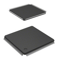
HD6417706F133 Renesas Electronics America, HD6417706F133 Datasheet - Page 247

HD6417706F133
Manufacturer Part Number
HD6417706F133
Description
IC SUPERH MPU ROMLESS 176LQFP
Manufacturer
Renesas Electronics America
Series
SuperH® SH7700r
Datasheet
1.HD6417706F133V.pdf
(751 pages)
Specifications of HD6417706F133
Core Processor
SH-3
Core Size
32-Bit
Speed
133MHz
Connectivity
EBI/EMI, FIFO, SCI, SmartCard
Peripherals
DMA, POR, WDT
Number Of I /o
103
Program Memory Type
ROMless
Ram Size
16K x 8
Voltage - Supply (vcc/vdd)
1.75 V ~ 2.05 V
Oscillator Type
Internal
Operating Temperature
-20°C ~ 75°C
Package / Case
176-LQFP
Lead Free Status / RoHS Status
Contains lead / RoHS non-compliant
Eeprom Size
-
Program Memory Size
-
Data Converters
-
Available stocks
Company
Part Number
Manufacturer
Quantity
Price
Part Number:
HD6417706F133
Manufacturer:
RENESAS/瑞萨
Quantity:
20 000
Company:
Part Number:
HD6417706F133V
Manufacturer:
EDISON
Quantity:
2 000
Company:
Part Number:
HD6417706F133V
Manufacturer:
Renesas Electronics America
Quantity:
10 000
Part Number:
HD6417706F133V
Manufacturer:
RENESAS/瑞萨
Quantity:
20 000
- Current page: 247 of 751
- Download datasheet (5Mb)
8.4.11
The refresh count register (RFCR) is a 16-bit read/write register. It is a 10-bit counter that
increments every time RTCOR and RTCNT match. When RFCR exceeds the count limit value set
in the LMTS of RTCSR, RTCSR's OVF bit is set and RFCR clears. RFCR is initialized to H'0000
when a power-on reset is performed. It is not initialized by a manual reset or standby mode, but
holds its contents.
Note: Writing to the RFCR differs from that to general registers to ensure the RFCR is not
8.5
8.5.1
This LSI supports both big endian, in which the 0 address is the most significant byte in the byte
data, and little endian, in which the 0 address is the least significant byte. This switchover is
designated by an external pin (MD5 pin) at the time of a power-on reset. After a power-on reset,
big endian is engaged when MD5 is low; little endian is engaged when MD5 is high.
Three data bus widths are available for ordinary memory (byte, word, longword) and two data bus
widths (word and longword) for synchronous DRAM. For the PCMCIA interface, choose from
byte and word. This means data alignment is done by matching the device's data width and endian.
The access unit must also be matched to the device's bus width. This also means that when
longword data is read from a byte-width device, the read operation must happen 4 times. In this
LSI, data alignment and conversion of data length is performed automatically between the
respective interfaces.
Tables 8.11 through 8.16 show the relationship between endian, device data width, and access
unit.
Bit
15 to 10
9 to 0
rewritten incorrectly. Use the word-transfer instruction to set the MSB and followed six
bits of upper bytes as B'101001 and remaining bits as the write data. For the byte-transfer
instruction, writing is disabled. Read data in 16 bits. 0 is read from undefined bits.
Refresh Count Register (RFCR)
Operation
Endian/Access Size and Data Alignment
Bit Name
—
—
Initial Value
All 0
All 0
R/W
R
R/W
Description
Reserved
These bits are always read as 0.
10-bit counter
Rev. 5.00 May 29, 2006 page 197 of 698
Section 8 Bus State Controller (BSC)
REJ09B0146-0500
Related parts for HD6417706F133
Image
Part Number
Description
Manufacturer
Datasheet
Request
R

Part Number:
Description:
KIT STARTER FOR M16C/29
Manufacturer:
Renesas Electronics America
Datasheet:

Part Number:
Description:
KIT STARTER FOR R8C/2D
Manufacturer:
Renesas Electronics America
Datasheet:

Part Number:
Description:
R0K33062P STARTER KIT
Manufacturer:
Renesas Electronics America
Datasheet:

Part Number:
Description:
KIT STARTER FOR R8C/23 E8A
Manufacturer:
Renesas Electronics America
Datasheet:

Part Number:
Description:
KIT STARTER FOR R8C/25
Manufacturer:
Renesas Electronics America
Datasheet:

Part Number:
Description:
KIT STARTER H8S2456 SHARPE DSPLY
Manufacturer:
Renesas Electronics America
Datasheet:

Part Number:
Description:
KIT STARTER FOR R8C38C
Manufacturer:
Renesas Electronics America
Datasheet:

Part Number:
Description:
KIT STARTER FOR R8C35C
Manufacturer:
Renesas Electronics America
Datasheet:

Part Number:
Description:
KIT STARTER FOR R8CL3AC+LCD APPS
Manufacturer:
Renesas Electronics America
Datasheet:

Part Number:
Description:
KIT STARTER FOR RX610
Manufacturer:
Renesas Electronics America
Datasheet:

Part Number:
Description:
KIT STARTER FOR R32C/118
Manufacturer:
Renesas Electronics America
Datasheet:

Part Number:
Description:
KIT DEV RSK-R8C/26-29
Manufacturer:
Renesas Electronics America
Datasheet:

Part Number:
Description:
KIT STARTER FOR SH7124
Manufacturer:
Renesas Electronics America
Datasheet:

Part Number:
Description:
KIT STARTER FOR H8SX/1622
Manufacturer:
Renesas Electronics America
Datasheet:

Part Number:
Description:
KIT DEV FOR SH7203
Manufacturer:
Renesas Electronics America
Datasheet:


