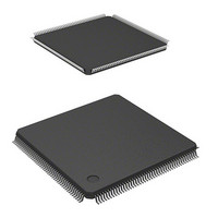
HD6417706F133 Renesas Electronics America, HD6417706F133 Datasheet - Page 479

HD6417706F133
Manufacturer Part Number
HD6417706F133
Description
IC SUPERH MPU ROMLESS 176LQFP
Manufacturer
Renesas Electronics America
Series
SuperH® SH7700r
Datasheet
1.HD6417706F133V.pdf
(751 pages)
Specifications of HD6417706F133
Core Processor
SH-3
Core Size
32-Bit
Speed
133MHz
Connectivity
EBI/EMI, FIFO, SCI, SmartCard
Peripherals
DMA, POR, WDT
Number Of I /o
103
Program Memory Type
ROMless
Ram Size
16K x 8
Voltage - Supply (vcc/vdd)
1.75 V ~ 2.05 V
Oscillator Type
Internal
Operating Temperature
-20°C ~ 75°C
Package / Case
176-LQFP
Lead Free Status / RoHS Status
Contains lead / RoHS non-compliant
Eeprom Size
-
Program Memory Size
-
Data Converters
-
Available stocks
Company
Part Number
Manufacturer
Quantity
Price
Part Number:
HD6417706F133
Manufacturer:
RENESAS/瑞萨
Quantity:
20 000
Company:
Part Number:
HD6417706F133V
Manufacturer:
EDISON
Quantity:
2 000
Company:
Part Number:
HD6417706F133V
Manufacturer:
Renesas Electronics America
Quantity:
10 000
Part Number:
HD6417706F133V
Manufacturer:
RENESAS/瑞萨
Quantity:
20 000
- Current page: 479 of 751
- Download datasheet (5Mb)
The operating sequence is:
1. The data line is high impedance when not in use and is fixed high with a pull-up resistor.
2. The transmitting side starts one frame of data transmission. The data frame starts with a start
3. On the smart card interface, the data line returns to high impedance after this. The data line is
4. The receiving side checks parity. When the data is received normally with no parity errors, the
5. The transmitting side transmits the next frame of data unless it receives an error signal. If it
15.4.4
Table 15.2 shows the bit map of the registers that the smart card interface uses. Bits shown as 1 or
0 must be set to the indicated value. The settings for the other bits are described below.
Table 15.2 Register Settings for the Smart Card Interface
Note: Dashes indicate unused bits.
1. Setting the serial mode register (SCSMR): The C/A bit selects the set timing of the TEND flag,
Register
SCSMR
SCBRR
SCSCR
SCTDR
SCSSR
SCRDR
SCSCMR H'FFFFFE8C
bit (Ds, low level). The start bit is followed by eight data bits (D0 to D7) and a parity bit (Dp).
pulled high with a pull-up resistor.
receiving side then waits to receive the next data. When a parity error occurs, the receiving
side outputs an error signal (DE, low level) and requests re-transfer of data. The receiving
station returns the signal line to high impedance after outputting the error signal for a specified
period. The signal line is pulled high with a pull-up resistor.
does receive an error signal, it returns to step 2 to re-transmit the erroneous data.
and selects the clock output state with the combination of bits CKE1 and CKE0 in the SCSCR.
Set the O/E bit to 0 when the IC card uses the direct convention or to 1 when it uses the inverse
convention. Select the on-chip baud rate generator clock source with the CKS1 and CKS0 bits
(see section 15.4.5, Clock).
Register Settings
Address
H'FFFFFE80
H'FFFFFE82
H'FFFFFE84
H'FFFFFE86
H'FFFFFE88
H'FFFFFE8A
Bit 7
C/A
BRR7
TIE
TDR7
TDRE
RDR7
—
Bit 6
0
BRR6
RIE
TDR6
RDRF
RDR6
—
Bit 5
1
BRR5
TE
TDR5
ORER
RDR5
—
Bit 4
O/E
BRR4
RE
TDR4
FER/
ERS
RDR4
—
Rev. 5.00 May 29, 2006 page 429 of 698
Bit 3
1
BRR3
0
TDR3
PER
RDR3
SDIR
Section 15 Smart Card Interface
Bit 2
0
BRR2
0
TDR2
TEND
RDR2
SINV
REJ09B0146-0500
Bit 1
CKS1
BRR1
CKE1
TDR1
0
RDR1
—
Bit 0
CKS0
BRR0
CKE0
TDR0
0
RDR0
SMIF
Related parts for HD6417706F133
Image
Part Number
Description
Manufacturer
Datasheet
Request
R

Part Number:
Description:
KIT STARTER FOR M16C/29
Manufacturer:
Renesas Electronics America
Datasheet:

Part Number:
Description:
KIT STARTER FOR R8C/2D
Manufacturer:
Renesas Electronics America
Datasheet:

Part Number:
Description:
R0K33062P STARTER KIT
Manufacturer:
Renesas Electronics America
Datasheet:

Part Number:
Description:
KIT STARTER FOR R8C/23 E8A
Manufacturer:
Renesas Electronics America
Datasheet:

Part Number:
Description:
KIT STARTER FOR R8C/25
Manufacturer:
Renesas Electronics America
Datasheet:

Part Number:
Description:
KIT STARTER H8S2456 SHARPE DSPLY
Manufacturer:
Renesas Electronics America
Datasheet:

Part Number:
Description:
KIT STARTER FOR R8C38C
Manufacturer:
Renesas Electronics America
Datasheet:

Part Number:
Description:
KIT STARTER FOR R8C35C
Manufacturer:
Renesas Electronics America
Datasheet:

Part Number:
Description:
KIT STARTER FOR R8CL3AC+LCD APPS
Manufacturer:
Renesas Electronics America
Datasheet:

Part Number:
Description:
KIT STARTER FOR RX610
Manufacturer:
Renesas Electronics America
Datasheet:

Part Number:
Description:
KIT STARTER FOR R32C/118
Manufacturer:
Renesas Electronics America
Datasheet:

Part Number:
Description:
KIT DEV RSK-R8C/26-29
Manufacturer:
Renesas Electronics America
Datasheet:

Part Number:
Description:
KIT STARTER FOR SH7124
Manufacturer:
Renesas Electronics America
Datasheet:

Part Number:
Description:
KIT STARTER FOR H8SX/1622
Manufacturer:
Renesas Electronics America
Datasheet:

Part Number:
Description:
KIT DEV FOR SH7203
Manufacturer:
Renesas Electronics America
Datasheet:


