MC56F8245VLD Freescale Semiconductor, MC56F8245VLD Datasheet - Page 388
MC56F8245VLD
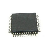
Manufacturer Part Number
MC56F8245VLD
Description
DSC 48K FLASH 60MHZ 44-LQFP
Manufacturer
Freescale Semiconductor
Series
56F8xxxr
Datasheets
1.TWR-56F8257.pdf
(88 pages)
2.MC56F8245VLD.pdf
(14 pages)
3.MC56F8245VLD.pdf
(2 pages)
4.MC56F8245VLD.pdf
(629 pages)
Specifications of MC56F8245VLD
Core Processor
56800E
Core Size
16-Bit
Speed
60MHz
Connectivity
CAN, I²C, LIN, SCI, SPI
Peripherals
LVD, POR, PWM, WDT
Number Of I /o
35
Program Memory Size
48KB (24K x 16)
Program Memory Type
FLASH
Ram Size
3K x 16
Voltage - Supply (vcc/vdd)
3 V ~ 3.6 V
Data Converters
A/D 8x12b, D/A 1x12b
Oscillator Type
Internal
Operating Temperature
-40°C ~ 105°C
Package / Case
44-LQFP
Product
DSCs
Processor Series
56800E
Core
56800E
Device Million Instructions Per Second
60 MIPs
Maximum Clock Frequency
60 MHz
Number Of Programmable I/os
35
Data Ram Size
6 KB
Operating Supply Voltage
3.3 V
Maximum Operating Temperature
+ 105 C
Mounting Style
SMD/SMT
Minimum Operating Temperature
- 40 C
On-chip Adc
12 bit, 4 Channel
Package
44LQFP
Family Name
MC56F82xx
Maximum Speed
60 MHz
Data Bus Width
16 Bit
Interface Type
I2C/SCI/SPI
On-chip Dac
1-chx12-bit
Number Of Timers
8
Lead Free Status / RoHS Status
Lead free / RoHS Compliant
Eeprom Size
-
Lead Free Status / Rohs Status
Details
Available stocks
Company
Part Number
Manufacturer
Quantity
Price
Company:

Part Number:
MC56F8245VLD
Manufacturer:
FREESCAL
Quantity:
269
Company:
Part Number:
MC56F8245VLD
Manufacturer:
Freescale Semiconductor
Quantity:
10 000


Signal Descriptions
12.2.1.3 SCLK (Serial Clock)
The serial clock synchronizes data transactions between master and slave devices. In a
master DSC, the SCLK pin is the clock output. In a slave DSC, the SCLK pin is the clock
input. In full duplex operation, the master and slave DSC exchange data in the same
number of clock cycles as the number of bits of transmitted data.
>
12.2.1.4 SS (Slave Select)
The SS pin has various functions depending on the current state of the SPI. For an SPI
configured as a slave, the SS is used to select a slave. For CPHA = 0, the SS is used to
define the start of a transaction. Because it is used to indicate the start of a transaction,
the SS must be toggled high and low between each full length set of data transmitted for
the CPHA = 0 format. However, it can remain low between transactions for the CPHA =
1 format.
When an SPI is configured as a slave, the SS pin is always configured as an input. The
MODFEN bit can prevent the state of the SS from creating a MODF error.
When an SPI is configured as a master, the SS input can be used in conjunction with the
MODF flag to prevent multiple masters from driving MOSI and SCLK. For the state of
the SS pin to set the MODF flag, the MODFEN bit in the SCTRL register must be set.
1. X = don't care
388
SPE
0
1
1
1
SPMSTR
A logic one voltage on the SS pin of a slave SPI puts the MISO
pin in a high-impedance state. The slave SPI ignores all
incoming SCLK clocks, even if it is already in the middle of a
transaction. A mode fault occurs if the SS pin changes state
during a transaction.
X
0
1
1
1
MC56F825x/4x Reference Manual, Rev. 2, 10/2010
MODFEN
X
X
0
1
Table 12-2. SPI IO Configuration
Not Enabled
Slave
Master without MODF
Master with MODF
SPI CONFIGURATION
Preliminary
NOTE
SS ignored by SPI
Input-only to SPI
SS input ignored by SPI, SS output
may be activated under software or
hardware control to select slave de‐
vices.
Input-only to SPI
STATE OF SS_B LOGIC
Freescale Semiconductor
Related parts for MC56F8245VLD
Image
Part Number
Description
Manufacturer
Datasheet
Request
R

Part Number:
Description:
Manufacturer:
Freescale Semiconductor, Inc
Datasheet:
Part Number:
Description:
Manufacturer:
Freescale Semiconductor, Inc
Datasheet:
Part Number:
Description:
Manufacturer:
Freescale Semiconductor, Inc
Datasheet:
Part Number:
Description:
Manufacturer:
Freescale Semiconductor, Inc
Datasheet:
Part Number:
Description:
Manufacturer:
Freescale Semiconductor, Inc
Datasheet:
Part Number:
Description:
Manufacturer:
Freescale Semiconductor, Inc
Datasheet:
Part Number:
Description:
Manufacturer:
Freescale Semiconductor, Inc
Datasheet:
Part Number:
Description:
Manufacturer:
Freescale Semiconductor, Inc
Datasheet:
Part Number:
Description:
Manufacturer:
Freescale Semiconductor, Inc
Datasheet:
Part Number:
Description:
Manufacturer:
Freescale Semiconductor, Inc
Datasheet:
Part Number:
Description:
Manufacturer:
Freescale Semiconductor, Inc
Datasheet:
Part Number:
Description:
Manufacturer:
Freescale Semiconductor, Inc
Datasheet:
Part Number:
Description:
Manufacturer:
Freescale Semiconductor, Inc
Datasheet:
Part Number:
Description:
Manufacturer:
Freescale Semiconductor, Inc
Datasheet:
Part Number:
Description:
Manufacturer:
Freescale Semiconductor, Inc
Datasheet: