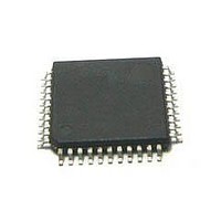
MC56F8245VLD Freescale Semiconductor, MC56F8245VLD Datasheet - Page 390

MC56F8245VLD
Manufacturer Part Number
MC56F8245VLD
Description
DSC 48K FLASH 60MHZ 44-LQFP
Manufacturer
Freescale Semiconductor
Series
56F8xxxr
Datasheets
1.TWR-56F8257.pdf
(88 pages)
2.MC56F8245VLD.pdf
(14 pages)
3.MC56F8245VLD.pdf
(2 pages)
4.MC56F8245VLD.pdf
(629 pages)
Specifications of MC56F8245VLD
Core Processor
56800E
Core Size
16-Bit
Speed
60MHz
Connectivity
CAN, I²C, LIN, SCI, SPI
Peripherals
LVD, POR, PWM, WDT
Number Of I /o
35
Program Memory Size
48KB (24K x 16)
Program Memory Type
FLASH
Ram Size
3K x 16
Voltage - Supply (vcc/vdd)
3 V ~ 3.6 V
Data Converters
A/D 8x12b, D/A 1x12b
Oscillator Type
Internal
Operating Temperature
-40°C ~ 105°C
Package / Case
44-LQFP
Product
DSCs
Processor Series
56800E
Core
56800E
Device Million Instructions Per Second
60 MIPs
Maximum Clock Frequency
60 MHz
Number Of Programmable I/os
35
Data Ram Size
6 KB
Operating Supply Voltage
3.3 V
Maximum Operating Temperature
+ 105 C
Mounting Style
SMD/SMT
Minimum Operating Temperature
- 40 C
On-chip Adc
12 bit, 4 Channel
Package
44LQFP
Family Name
MC56F82xx
Maximum Speed
60 MHz
Data Bus Width
16 Bit
Interface Type
I2C/SCI/SPI
On-chip Dac
1-chx12-bit
Number Of Timers
8
Lead Free Status / RoHS Status
Lead free / RoHS Compliant
Eeprom Size
-
Lead Free Status / Rohs Status
Details
Available stocks
Company
Part Number
Manufacturer
Quantity
Price
Company:
Part Number:
MC56F8245VLD
Manufacturer:
FREESCAL
Quantity:
269
Company:
Part Number:
MC56F8245VLD
Manufacturer:
Freescale Semiconductor
Quantity:
10 000
- TWR-56F8257 PDF datasheet
- MC56F8245VLD PDF datasheet #2
- MC56F8245VLD PDF datasheet #3
- MC56F8245VLD PDF datasheet #4
- Current page: 390 of 629
- Download datasheet (4Mb)
Memory Map Registers
Address: QSPI0_SCTRL – F200h base + 0h offset = F200h
390
Reset
Read
Write
Bit
MODFEN
ERRIE
15–13
DSO
Field
SPR
12
11
10
15
0
SPR
14
1
SPI Baud Rate Select
In master mode, these read/write bits select one of four baud rates. SPR1 and SPR0 have no effect in
slave mode. Reset sets SPR[2:0] to b011.
Use the following formula to calculate the SPI baud rate:
Baud rate = clk/BD
00
01
10
11
Data Shift Order
This read/write bit determines which bit is transmitted or received first, either the MSB or LSB. Both
master and slave SPI modules need to transmit and receive the same length packets. Regardless of how
this bit is set, when reading the from the QSPI0_DRCV or writing to the QSPI0_DXMIT the LSB will
always be at bit location 0 and the MSB will at the correct bit position. If the data length is less than 16
bits, the data will be zero padded on the upper bits.
0
1
Error Interrupt Enable
This read/write bit enables the MODF (if MODFEN is also set) and OVRF bits to generate DSC interrupt
requests. Reset clears the ERRIE bit.
0
1
Mode Fault Enable
This read/write bit, when set to 1, allows the MODF flag to be set. If the MODF flag is set, clearing the
MODFEN does not clear the MODF flag.
If the MODFEN bit is low, the level of the SS_B pin does not affect the operation of an enabled SPI
configured as a master. If configured as a master and MODFEN=1, a transaction in progress will stop if
SS_B goes low.
For an enabled SPI configured as a slave, having MODFEN low only prevents the MODF flag from being
set. It does not affect any other part of SPI operation.
MSB transmitted first (MSB -> LSB)
LSB transmitted first (LSB -> MSB)
MODF and OVRF cannot generate DSC interrupt requests
MODF and OVRF can generate DSC interrupt requests
13
Baud rate divisor 2
Baud rate divisor 4
Baud rate divisor 8
Baud rate divisor 16
1
DSO
12
0
MC56F825x/4x Reference Manual, Rev. 2, 10/2010
11
QSPI0_SCTRL field descriptions
0
where: clk= Peripheral Bus Clock
Table continues on the next page...
10
0
0
9
Preliminary
BD = baud rate divisor
1
8
Description
CPOL
0
7
1
6
SPE
0
5
0
4
SPRF OVRF
0
3
Freescale Semiconductor
0
2
MOD
F
0
1
SPTE
1
0
Related parts for MC56F8245VLD
Image
Part Number
Description
Manufacturer
Datasheet
Request
R
Part Number:
Description:
Manufacturer:
Freescale Semiconductor, Inc
Datasheet:
Part Number:
Description:
Manufacturer:
Freescale Semiconductor, Inc
Datasheet:
Part Number:
Description:
Manufacturer:
Freescale Semiconductor, Inc
Datasheet:
Part Number:
Description:
Manufacturer:
Freescale Semiconductor, Inc
Datasheet:
Part Number:
Description:
Manufacturer:
Freescale Semiconductor, Inc
Datasheet:
Part Number:
Description:
Manufacturer:
Freescale Semiconductor, Inc
Datasheet:
Part Number:
Description:
Manufacturer:
Freescale Semiconductor, Inc
Datasheet:
Part Number:
Description:
Manufacturer:
Freescale Semiconductor, Inc
Datasheet:
Part Number:
Description:
Manufacturer:
Freescale Semiconductor, Inc
Datasheet:
Part Number:
Description:
Manufacturer:
Freescale Semiconductor, Inc
Datasheet:
Part Number:
Description:
Manufacturer:
Freescale Semiconductor, Inc
Datasheet:
Part Number:
Description:
Manufacturer:
Freescale Semiconductor, Inc
Datasheet:
Part Number:
Description:
Manufacturer:
Freescale Semiconductor, Inc
Datasheet:
Part Number:
Description:
Manufacturer:
Freescale Semiconductor, Inc
Datasheet:
Part Number:
Description:
Manufacturer:
Freescale Semiconductor, Inc
Datasheet:


