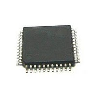
MC56F8245VLD Freescale Semiconductor, MC56F8245VLD Datasheet - Page 78

MC56F8245VLD
Manufacturer Part Number
MC56F8245VLD
Description
DSC 48K FLASH 60MHZ 44-LQFP
Manufacturer
Freescale Semiconductor
Series
56F8xxxr
Datasheets
1.TWR-56F8257.pdf
(88 pages)
2.MC56F8245VLD.pdf
(14 pages)
3.MC56F8245VLD.pdf
(2 pages)
4.MC56F8245VLD.pdf
(629 pages)
Specifications of MC56F8245VLD
Core Processor
56800E
Core Size
16-Bit
Speed
60MHz
Connectivity
CAN, I²C, LIN, SCI, SPI
Peripherals
LVD, POR, PWM, WDT
Number Of I /o
35
Program Memory Size
48KB (24K x 16)
Program Memory Type
FLASH
Ram Size
3K x 16
Voltage - Supply (vcc/vdd)
3 V ~ 3.6 V
Data Converters
A/D 8x12b, D/A 1x12b
Oscillator Type
Internal
Operating Temperature
-40°C ~ 105°C
Package / Case
44-LQFP
Product
DSCs
Processor Series
56800E
Core
56800E
Device Million Instructions Per Second
60 MIPs
Maximum Clock Frequency
60 MHz
Number Of Programmable I/os
35
Data Ram Size
6 KB
Operating Supply Voltage
3.3 V
Maximum Operating Temperature
+ 105 C
Mounting Style
SMD/SMT
Minimum Operating Temperature
- 40 C
On-chip Adc
12 bit, 4 Channel
Package
44LQFP
Family Name
MC56F82xx
Maximum Speed
60 MHz
Data Bus Width
16 Bit
Interface Type
I2C/SCI/SPI
On-chip Dac
1-chx12-bit
Number Of Timers
8
Lead Free Status / RoHS Status
Lead free / RoHS Compliant
Eeprom Size
-
Lead Free Status / Rohs Status
Details
Available stocks
Company
Part Number
Manufacturer
Quantity
Price
Company:
Part Number:
MC56F8245VLD
Manufacturer:
FREESCAL
Quantity:
269
Company:
Part Number:
MC56F8245VLD
Manufacturer:
Freescale Semiconductor
Quantity:
10 000
- TWR-56F8257 PDF datasheet
- MC56F8245VLD PDF datasheet #2
- MC56F8245VLD PDF datasheet #3
- MC56F8245VLD PDF datasheet #4
- Current page: 78 of 629
- Download datasheet (4Mb)
Memory Map and Registers
2.3.22 ADC Scan Control Register (ADC_SCTRL)
This register is an extension to the CLIST1-4 registers, providing the ability to pause and
await a new sync while processing samples programmed in the CLIST*[SAMPLE0–
SAMPLE15] fields.
These 16 control bits are used to determine whether a sample in a scan occurs
immediately or if the sample waits for an enabled sync input to occur. The sync input
must occur after the conversion of the current sample completes. During sequential mode
scans, the SCTRL[SC] bits are used in order from SC0 to SC15. During simultaneous
parallel scan modes, the bits are used in order from SC0 to SC7. In non-simultaneous
parallel scans, ADCA uses the bits in order from SC0 to SC3 followed by SC8 to SC11.
ADCB will use bits SC4 to SC7 followed by SC12 to SC15 in non-simultaneous parallel
scans.
When setting SCTRL[SC0], don’t set CTRL1[START0] or CTRL2[START1]. Just clear
CTRL1[STOP0] or CTRL2[STOP1] and the first enabled sync input will start the scan.
Setting SC0 delays sample 0 until a sync pulse occurs. Setting SC1 delays sample 1 until
a sync pulse occurs after completing sample 0.
Address: ADC_SCTRL – F080h base + 38h offset = F0B8h
78
Reset
Read
Write
Bit
SC[15:0]
15–0
Field
Field
15
0
14
0
01
10
11
Scan Control Bits
0
1
Perform sample immediately after the completion of the current sample.
Delay sample until a new sync input occurs.
x2 amplification
x4 amplification
reserved
13
0
12
0
MC56F825x/4x Reference Manual, Rev. 2, 10/2010
ADC_GC2 field descriptions (continued)
11
0
ADC_SCTRL field descriptions
10
0
0
9
Preliminary
SC[15:0]
0
8
Description
Description
0
7
0
6
0
5
0
4
0
3
Freescale Semiconductor
0
2
0
1
0
0
Related parts for MC56F8245VLD
Image
Part Number
Description
Manufacturer
Datasheet
Request
R
Part Number:
Description:
Manufacturer:
Freescale Semiconductor, Inc
Datasheet:
Part Number:
Description:
Manufacturer:
Freescale Semiconductor, Inc
Datasheet:
Part Number:
Description:
Manufacturer:
Freescale Semiconductor, Inc
Datasheet:
Part Number:
Description:
Manufacturer:
Freescale Semiconductor, Inc
Datasheet:
Part Number:
Description:
Manufacturer:
Freescale Semiconductor, Inc
Datasheet:
Part Number:
Description:
Manufacturer:
Freescale Semiconductor, Inc
Datasheet:
Part Number:
Description:
Manufacturer:
Freescale Semiconductor, Inc
Datasheet:
Part Number:
Description:
Manufacturer:
Freescale Semiconductor, Inc
Datasheet:
Part Number:
Description:
Manufacturer:
Freescale Semiconductor, Inc
Datasheet:
Part Number:
Description:
Manufacturer:
Freescale Semiconductor, Inc
Datasheet:
Part Number:
Description:
Manufacturer:
Freescale Semiconductor, Inc
Datasheet:
Part Number:
Description:
Manufacturer:
Freescale Semiconductor, Inc
Datasheet:
Part Number:
Description:
Manufacturer:
Freescale Semiconductor, Inc
Datasheet:
Part Number:
Description:
Manufacturer:
Freescale Semiconductor, Inc
Datasheet:
Part Number:
Description:
Manufacturer:
Freescale Semiconductor, Inc
Datasheet:


