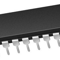
PIC16F1829-E/P Microchip Technology, PIC16F1829-E/P Datasheet - Page 104

PIC16F1829-E/P
Manufacturer Part Number
PIC16F1829-E/P
Description
14 KB Flash, 1K Bytes RAM, 32 MHz Int. Osc, 18 I/0, Enhanced Mid Range Core 20 P
Manufacturer
Microchip Technology
Series
PIC® XLP™ mTouch™ 16Fr
Datasheet
1.PIC16LF1829-ISO.pdf
(420 pages)
Specifications of PIC16F1829-E/P
Core Processor
PIC
Core Size
8-Bit
Speed
32MHz
Connectivity
I²C, LIN, SPI, UART/USART
Peripherals
Brown-out Detect/Reset, POR, PWM, WDT
Number Of I /o
17
Program Memory Size
14KB (8K x 14)
Program Memory Type
FLASH
Eeprom Size
256 x 8
Ram Size
1K x 8
Voltage - Supply (vcc/vdd)
1.8 V ~ 5.5 V
Data Converters
A/D 12x10b
Oscillator Type
Internal
Operating Temperature
-40°C ~ 125°C
Package / Case
*
Processor Series
PIC16F182x
Core
PIC
Data Bus Width
8 bit
Data Ram Size
1 KB
Interface Type
I2C, SPI, USART
Maximum Clock Frequency
32 MHz
Number Of Programmable I/os
18
Number Of Timers
5
Operating Supply Voltage
1.8 V to 5.5 V
Maximum Operating Temperature
+ 125 C
Mounting Style
Through Hole
Lead Free Status / RoHS Status
Lead free / RoHS Compliant
Lead Free Status / RoHS Status
Lead free / RoHS Compliant
- Current page: 104 of 420
- Download datasheet (5Mb)
PIC16F/LF1825/1829
Even if the flag bits were checked before executing a
SLEEP instruction, it may be possible for flag bits to
become set before the SLEEP instruction completes. To
determine whether a SLEEP instruction executed, test
the PD bit. If the PD bit is set, the SLEEP instruction
was executed as a NOP.
FIGURE 9-1:
TABLE 9-1:
DS41440A-page 104
Name
INTCON
IOCAF
IOCAN
IOCAP
IOCBF
IOCBN
IOCBP
PIE1
PIE2
PIE4
PIR1
PIR2
PIR4
STATUS
WDTCON
Legend:
Note
Instruction Flow
(INTCON reg.)
Note
Interrupt flag
GIE bit
Instruction
Fetched
Instruction
Executed
CLKOUT
(1)
(1)
(1)
(1)
OSC1
(1)
1:
1:
2:
3:
4:
PC
(1)
(2)
— = unimplemented, read as ‘0’. Shaded cells are not used in Power-down mode.
PIC16F/LF1829 only.
XT, HS or LP Oscillator mode assumed.
CLKOUT is not available in XT, HS, or LP Oscillator modes, but shown here for timing reference.
T
GIE = 1 assumed. In this case after wake-up, the processor calls the ISR at 0004h. If GIE = 0, execution will continue in-line.
TMR1GIE
TMR1GIF
OST
Q1 Q2 Q3 Q4 Q1 Q2 Q3 Q4 Q1
IOCBN7
IOCBP7
Inst(PC) = Sleep
IOCBF7
OSFIE
OSFIF
Bit 7
GIE
Inst(PC - 1)
—
—
—
—
—
—
—
= 1024 T
SUMMARY OF REGISTERS ASSOCIATED WITH POWER-DOWN MODE
PC
WAKE-UP FROM SLEEP THROUGH INTERRUPT
OSC
IOCBF6
IOCBN6
IOCBP6
PEIE
ADIE
ADIF
Bit 6
C2IE
C2IF
(drawing not to scale). This delay applies only to XT, HS or LP Oscillator modes.
—
—
—
—
—
—
—
Inst(PC + 1)
Sleep
PC + 1
WDTPS4
TMR0IE
IOCAN5
IOCAP5
IOCBN5
IOCBP5
IOCAF5
IOCBF5
RCIE
RCIF
Bit 5
C1IE
C1IF
—
—
—
Processor in
Sleep
WDTPS3
IOCAN4
IOCBN4
IOCAF4
IOCAP4
IOCBF4
IOCBP4
PC + 2
Bit 4
INTE
TXIE
EEIE
TXIF
EEIF
TO
Preliminary
—
—
T
OST (3)
WDTPS2
Q1 Q2 Q3 Q4 Q1 Q2 Q3 Q4 Q1 Q2 Q3 Q4 Q1 Q2 Q3 Q4
IOCAF3
IOCAN3
IOCAP3
SSP1IE
BCL1IE
SSP1IF
BCL1IF
IOCIE
Bit 3
Interrupt Latency
Inst(PC + 2)
Inst(PC + 1)
PD
—
—
—
—
—
PC + 2
WDTPS1
IOCAN2
IOCAP2
TMR0IF
IOCAF2
CCP1IE
CCP1IF
Bit 2
—
—
—
—
—
—
—
Z
(4)
Dummy Cycle
PC + 2
WDTPS0
IOCAN1
IOCAF1
IOCAP1
TMR2IE
TMR2IF
BCL2IE
BCL2IF
Bit 1
INTF
DC
—
—
—
—
—
2010 Microchip Technology Inc.
Dummy Cycle
Inst(0004h)
0004h
SWDTEN
IOCAF0
IOCAN0
IOCAP0
TMR1IE
CCP2IE
TMR1IF
SSP2IE
CCP2IF
SSP2IF
IOCIF
Bit 0
—
—
—
C
Inst(0005h)
Inst(0004h)
0005h
Register on
Page
144
144
144
146
145
145
101
107
93
94
95
97
98
99
26
Related parts for PIC16F1829-E/P
Image
Part Number
Description
Manufacturer
Datasheet
Request
R

Part Number:
Description:
IC, 8BIT MCU, PIC16F, 32MHZ, SOIC-18
Manufacturer:
Microchip Technology
Datasheet:

Part Number:
Description:
IC, 8BIT MCU, PIC16F, 32MHZ, SSOP-20
Manufacturer:
Microchip Technology
Datasheet:

Part Number:
Description:
IC, 8BIT MCU, PIC16F, 32MHZ, DIP-18
Manufacturer:
Microchip Technology
Datasheet:

Part Number:
Description:
IC, 8BIT MCU, PIC16F, 32MHZ, QFN-28
Manufacturer:
Microchip Technology
Datasheet:

Part Number:
Description:
IC, 8BIT MCU, PIC16F, 32MHZ, QFN-28
Manufacturer:
Microchip Technology
Datasheet:

Part Number:
Description:
IC, 8BIT MCU, PIC16F, 32MHZ, QFN-28
Manufacturer:
Microchip Technology
Datasheet:

Part Number:
Description:
IC, 8BIT MCU, PIC16F, 32MHZ, SSOP-20
Manufacturer:
Microchip Technology
Datasheet:

Part Number:
Description:
IC, 8BIT MCU, PIC16F, 20MHZ, DIP-40
Manufacturer:
Microchip Technology
Datasheet:

Part Number:
Description:
IC, 8BIT MCU, PIC16F, 32MHZ, QFN-28
Manufacturer:
Microchip Technology
Datasheet:

Part Number:
Description:
IC, 8BIT MCU, PIC16F, 20MHZ, MQFP-44
Manufacturer:
Microchip Technology
Datasheet:

Part Number:
Description:
IC, 8BIT MCU, PIC16F, 20MHZ, QFN-20
Manufacturer:
Microchip Technology
Datasheet:

Part Number:
Description:
IC, 8BIT MCU, PIC16F, 32MHZ, QFN-28
Manufacturer:
Microchip Technology
Datasheet:

Part Number:
Description:
MCU 14KB FLASH 768B RAM 64-TQFP
Manufacturer:
Microchip Technology
Datasheet:

Part Number:
Description:
7 KB Flash, 384 Bytes RAM, 32 MHz Int. Osc, 16 I/0, Enhanced Mid Range Core, Low
Manufacturer:
Microchip Technology

Part Number:
Description:
14KB Flash, 512B RAM, 256B EEPROM, LCD, 1.8-5.5V 40 UQFN 5x5x0.5mm TUBE
Manufacturer:
Microchip Technology
Datasheet:


