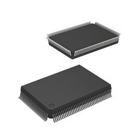
DF2367VF33 Renesas Electronics America, DF2367VF33 Datasheet - Page 15

DF2367VF33
Manufacturer Part Number
DF2367VF33
Description
MCU 3V 384K 128-QFP
Manufacturer
Renesas Electronics America
Series
H8® H8S/2300r
Datasheet
1.DF2368VTE34V.pdf
(1044 pages)
Specifications of DF2367VF33
Core Processor
H8S/2000
Core Size
16-Bit
Speed
33MHz
Connectivity
I²C, IrDA, SCI, SmartCard
Peripherals
DMA, POR, PWM, WDT
Number Of I /o
84
Program Memory Size
384KB (384K x 8)
Program Memory Type
FLASH
Ram Size
24K x 8
Voltage - Supply (vcc/vdd)
3 V ~ 3.6 V
Data Converters
A/D 10x10b, D/A 2x8b
Oscillator Type
Internal
Operating Temperature
-20°C ~ 75°C
Package / Case
128-QFP
Lead Free Status / RoHS Status
Contains lead / RoHS non-compliant
Eeprom Size
-
Other names
HD64F2367VF33
HD64F2367VF33
HD64F2367VF33
Available stocks
Company
Part Number
Manufacturer
Quantity
Price
Company:
Part Number:
DF2367VF33V
Manufacturer:
Renesas Electronics America
Quantity:
135
Company:
Part Number:
DF2367VF33V
Manufacturer:
Renesas Electronics America
Quantity:
10 000
Company:
Part Number:
DF2367VF33WV
Manufacturer:
Renesas Electronics America
Quantity:
10 000
- Current page: 15 of 1044
- Download datasheet (6Mb)
Item
15.3.1 I
Register A (ICCRA)
Table 15.2 Transfer Rate
15.3.5 I
Register (ICSR)
15.4.5 Slave Receive
Operation
Figure 15.12 Slave
Receive Mode Operation
Timing 2
15.4.7 Example of Use
Figure 15.14 Sample
Flowchart for Master
Transmit Mode
2
2
C Bus Control
C Bus Status
Page Revision (See Manual for Details)
634
639
652
654
Note amended
Notes: 2. Does not conform to the I
Table amended
Figure amended
(master output)
Figure amended
(master output)
Bit Bit Name
7
(slave output)
(slave output)
processing
ICDRS
ICDRR
RDRF
SCL
SDA
SCL
SDA
User
TDRE
No
Read BBSY in ICCRB
Set MST = 1 and TRS
Write BBSY = 1
= 1 in ICCRA.
and SCP = 0.
BBSY=0 ?
Initialize
Start
specification (standard mode: max. 100 kHz, fast
mode: max. 400 kHz).
Initial Value R/W
0
Yes
A
9
Bit 7
1
R/W
Bit 6
Data 1
2
[1]
[2]
[3]
Rev.6.00 Mar. 18, 2009 Page xiii of lviii
Transmit Data Register Empty
Bit 5
Description
[Setting conditions]
•
•
•
[Clearing conditions]
•
•
3
When data is transferred from ICDRT to ICDRS and
ICDRT becomes empty
When TRS is set
When a transition from receive mode to transmit mode is
made in slave mode
When 0 is written in TDRE after reading TDRE = 1
When data is written to ICDRT
[1]
[2]
[3]
[4]
Note: * Ensure that no interrupts occur between
Bit 4
4
Test the status of the SCL and SDA lines.*
Select master transmit mode.*
Start condition issuance.*
Select transmit data for the first byte (slave address + R/W),
and clear TDRE to 0.
[7] Set ACKBT
Bit 3
when BBSY is cleared to 0 and start condition [3].
5
2
C bus interface
Bit 2
6
Bit 1
7
[8] Read ICDRR,
and clear RDRF.
REJ09B0050-0600
Bit 0
8
A
9
[10] Read ICDRR,
and clear RDRF.
Data 1
Data 2
Related parts for DF2367VF33
Image
Part Number
Description
Manufacturer
Datasheet
Request
R

Part Number:
Description:
CONN PLUG 12POS DUAL 0.5MM SMD
Manufacturer:
Hirose Electric Co Ltd
Datasheet:

Part Number:
Description:
CONN PLUG 18POS DUAL 0.5MM SMD
Manufacturer:
Hirose Electric Co Ltd
Datasheet:

Part Number:
Description:
CONN PLUG 14POS DUAL 0.5MM SMD
Manufacturer:
Hirose Electric Co Ltd
Datasheet:

Part Number:
Description:
CONN RECEPT 20POS DUAL 0.5MM SMD
Manufacturer:
Hirose Electric Co Ltd
Datasheet:

Part Number:
Description:
CONN PLUG 16POS DUAL 0.5MM SMD
Manufacturer:
Hirose Electric Co Ltd
Datasheet:

Part Number:
Description:
CONN RECEPT 16POS DUAL 0.5MM SMD
Manufacturer:
Hirose Electric Co Ltd
Datasheet:

Part Number:
Description:
CONN PLUG 20POS DUAL 0.5MM SMD
Manufacturer:
Hirose Electric Co Ltd
Datasheet:

Part Number:
Description:
CONN PLUG 30POS DUAL 0.5MM SMD
Manufacturer:
Hirose Electric Co Ltd
Datasheet:

Part Number:
Description:
CONN RECEPT 30POS DUAL 0.5MM SMD
Manufacturer:
Hirose Electric Co Ltd
Datasheet:

Part Number:
Description:
CONN PLUG 40POS DUAL 0.5MM SMD
Manufacturer:
Hirose Electric Co Ltd
Datasheet:

Part Number:
Description:
KIT STARTER FOR M16C/29
Manufacturer:
Renesas Electronics America
Datasheet:

Part Number:
Description:
KIT STARTER FOR R8C/2D
Manufacturer:
Renesas Electronics America
Datasheet:

Part Number:
Description:
R0K33062P STARTER KIT
Manufacturer:
Renesas Electronics America
Datasheet:

Part Number:
Description:
KIT STARTER FOR R8C/23 E8A
Manufacturer:
Renesas Electronics America
Datasheet:

Part Number:
Description:
KIT STARTER FOR R8C/25
Manufacturer:
Renesas Electronics America
Datasheet:


