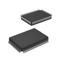
DF2367VF33 Renesas Electronics America, DF2367VF33 Datasheet - Page 49

DF2367VF33
Manufacturer Part Number
DF2367VF33
Description
MCU 3V 384K 128-QFP
Manufacturer
Renesas Electronics America
Series
H8® H8S/2300r
Datasheet
1.DF2368VTE34V.pdf
(1044 pages)
Specifications of DF2367VF33
Core Processor
H8S/2000
Core Size
16-Bit
Speed
33MHz
Connectivity
I²C, IrDA, SCI, SmartCard
Peripherals
DMA, POR, PWM, WDT
Number Of I /o
84
Program Memory Size
384KB (384K x 8)
Program Memory Type
FLASH
Ram Size
24K x 8
Voltage - Supply (vcc/vdd)
3 V ~ 3.6 V
Data Converters
A/D 10x10b, D/A 2x8b
Oscillator Type
Internal
Operating Temperature
-20°C ~ 75°C
Package / Case
128-QFP
Lead Free Status / RoHS Status
Contains lead / RoHS non-compliant
Eeprom Size
-
Other names
HD64F2367VF33
HD64F2367VF33
HD64F2367VF33
Available stocks
Company
Part Number
Manufacturer
Quantity
Price
Company:
Part Number:
DF2367VF33V
Manufacturer:
Renesas Electronics America
Quantity:
135
Company:
Part Number:
DF2367VF33V
Manufacturer:
Renesas Electronics America
Quantity:
10 000
Company:
Part Number:
DF2367VF33WV
Manufacturer:
Renesas Electronics America
Quantity:
10 000
- Current page: 49 of 1044
- Download datasheet (6Mb)
Figure 14.31 Timing for Fixing Clock Output Level................................................................... 614
Figure 14.32 Clock Halt and Restart Procedure .......................................................................... 615
Figure 14.33 Block Diagram of IrDA.......................................................................................... 616
Figure 14.34 IrDA Transmit/Receive Operations........................................................................ 617
Figure 14.35 Example of Synchronous Transmission Using DTC.............................................. 623
Figure 14.36 Sample Flowchart for Mode Transition during Transmission................................ 625
Figure 14.37 Port Pin States during Mode Transition (Internal Clock, Asynchronous
Figure 14.38 Port Pin States during Mode Transition (Internal Clock,
Figure 14.39 Sample Flowchart for Mode Transition during Reception ..................................... 627
Section 15 I
Figure 15.1 Block Diagram of I
Figure 15.2 External Circuit Connections of I/O Pins ............................................................... 631
Figure 15.3 I
Figure 15.4 I
Figure 15.5 Master Transmit Mode Operation Timing 1........................................................... 645
Figure 15.6 Master Transmit Mode Operation Timing 2........................................................... 646
Figure 15.7 Master Receive Mode Operation Timing 1 ............................................................ 647
Figure 15.8 Master Receive Mode Operation Timing 2 ............................................................ 648
Figure 15.9 Slave Transmit Mode Operation Timing 1............................................................. 649
Figure 15.10 Slave Transmit Mode Operation Timing 2............................................................. 650
Figure 15.11 Slave Receive Mode Operation Timing 1 .............................................................. 651
Figure 15.12 Slave Receive Mode Operation Timing 2 .............................................................. 652
Figure 15.13 Block Diagram of Noise Canceler.......................................................................... 653
Figure 15.14 Sample Flowchart for Master Transmit Mode........................................................ 654
Figure 15.15 Sample Flowchart for Master Receive Mode ......................................................... 655
Figure 15.16 Sample Flowchart for Slave Transmit Mode.......................................................... 656
Figure 15.17 Sample Flowchart for Slave Receive Mode ........................................................... 657
Figure 15.18 Timing of the Bit Synchronous Circuit .................................................................. 659
Section 16 A/D Converter................................................................................. 661
Figure 16.1 Block Diagram of A/D Converter ..........................................................................662
Figure 16.2 A/D Conversion Timing.........................................................................................671
Figure 16.3 External Trigger Input Timing ...............................................................................673
Figure 16.4 A/D Conversion Precision Definitions ...................................................................675
Figure 16.5 A/D Conversion Precision Definitions ...................................................................675
Figure 16.6 Example of Analog Input Circuit ...........................................................................676
Figure 16.7 Example of Analog Input Protection Circuit ..........................................................678
Synchronous Transmission) ................................................................................... 626
2
Transmission) ........................................................................................................ 626
C Bus Interface2 (IIC2) (Option)
2
2
C Bus Formats...................................................................................................... 643
C Bus Timing....................................................................................................... 643
2
C Bus Interface2..................................................................... 630
Rev.6.00 Mar. 18, 2009 Page xlvii of lviii
REJ09B0050-0600
Related parts for DF2367VF33
Image
Part Number
Description
Manufacturer
Datasheet
Request
R

Part Number:
Description:
CONN PLUG 12POS DUAL 0.5MM SMD
Manufacturer:
Hirose Electric Co Ltd
Datasheet:

Part Number:
Description:
CONN PLUG 18POS DUAL 0.5MM SMD
Manufacturer:
Hirose Electric Co Ltd
Datasheet:

Part Number:
Description:
CONN PLUG 14POS DUAL 0.5MM SMD
Manufacturer:
Hirose Electric Co Ltd
Datasheet:

Part Number:
Description:
CONN RECEPT 20POS DUAL 0.5MM SMD
Manufacturer:
Hirose Electric Co Ltd
Datasheet:

Part Number:
Description:
CONN PLUG 16POS DUAL 0.5MM SMD
Manufacturer:
Hirose Electric Co Ltd
Datasheet:

Part Number:
Description:
CONN RECEPT 16POS DUAL 0.5MM SMD
Manufacturer:
Hirose Electric Co Ltd
Datasheet:

Part Number:
Description:
CONN PLUG 20POS DUAL 0.5MM SMD
Manufacturer:
Hirose Electric Co Ltd
Datasheet:

Part Number:
Description:
CONN PLUG 30POS DUAL 0.5MM SMD
Manufacturer:
Hirose Electric Co Ltd
Datasheet:

Part Number:
Description:
CONN RECEPT 30POS DUAL 0.5MM SMD
Manufacturer:
Hirose Electric Co Ltd
Datasheet:

Part Number:
Description:
CONN PLUG 40POS DUAL 0.5MM SMD
Manufacturer:
Hirose Electric Co Ltd
Datasheet:

Part Number:
Description:
KIT STARTER FOR M16C/29
Manufacturer:
Renesas Electronics America
Datasheet:

Part Number:
Description:
KIT STARTER FOR R8C/2D
Manufacturer:
Renesas Electronics America
Datasheet:

Part Number:
Description:
R0K33062P STARTER KIT
Manufacturer:
Renesas Electronics America
Datasheet:

Part Number:
Description:
KIT STARTER FOR R8C/23 E8A
Manufacturer:
Renesas Electronics America
Datasheet:

Part Number:
Description:
KIT STARTER FOR R8C/25
Manufacturer:
Renesas Electronics America
Datasheet:


