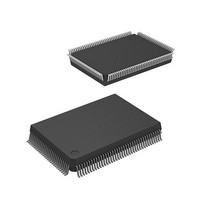
DF2367VF33 Renesas Electronics America, DF2367VF33 Datasheet - Page 896

DF2367VF33
Manufacturer Part Number
DF2367VF33
Description
MCU 3V 384K 128-QFP
Manufacturer
Renesas Electronics America
Series
H8® H8S/2300r
Datasheet
1.DF2368VTE34V.pdf
(1044 pages)
Specifications of DF2367VF33
Core Processor
H8S/2000
Core Size
16-Bit
Speed
33MHz
Connectivity
I²C, IrDA, SCI, SmartCard
Peripherals
DMA, POR, PWM, WDT
Number Of I /o
84
Program Memory Size
384KB (384K x 8)
Program Memory Type
FLASH
Ram Size
24K x 8
Voltage - Supply (vcc/vdd)
3 V ~ 3.6 V
Data Converters
A/D 10x10b, D/A 2x8b
Oscillator Type
Internal
Operating Temperature
-20°C ~ 75°C
Package / Case
128-QFP
Lead Free Status / RoHS Status
Contains lead / RoHS non-compliant
Eeprom Size
-
Other names
HD64F2367VF33
HD64F2367VF33
HD64F2367VF33
Available stocks
Company
Part Number
Manufacturer
Quantity
Price
Company:
Part Number:
DF2367VF33V
Manufacturer:
Renesas Electronics America
Quantity:
135
Company:
Part Number:
DF2367VF33V
Manufacturer:
Renesas Electronics America
Quantity:
10 000
Company:
Part Number:
DF2367VF33WV
Manufacturer:
Renesas Electronics America
Quantity:
10 000
- Current page: 896 of 1044
- Download datasheet (6Mb)
Section 23 Power-Down Modes
23.2.6
When the ACSE bit in MSTPCRH is set to 1 and module stop mode is set for all the on-chip
peripheral functions controlled by MSTPCR or EXMSTPCR (MSTPCR = H'FFFF, EXMSTPCR
= H'FFFF), or for all the on-chip peripheral functions except the 8-bit timer (MSTPCR = H'FFFE,
EXMSTPCR = H'FFFF), executing a SLEEP instruction while the SSBY bit in SBYCR is cleared
to 0 will cause all the on-chip peripheral functions (except the 8-bit timer and watchdog timer), the
bus controller, and the I/O ports to stop operating, and a transition to be made to all-module-
clocks-stop mode, at the end of the bus cycle.
Operation or halting of the 8-bit timer can be selected by means of the MSTP0 bit.
All-module-clocks-stop mode is cleared by an external interrupt (NMI, IRQ0 to IRQ7 pins), RES
pin input, or an internal interrupt (8-bit timer, watchdog timer), and the CPU returns to the normal
program execution state via the exception handling state. All-module-clocks-stop mode is not
cleared if interrupts are disabled, if interrupts other than NMI are masked by the CPU, or if the
relevant interrupt is designated as a DTC activation source.
When the STBY pin is driven low, a transition is made to hardware standby mode.
23.3
Output of the φ clock can be controlled by means of the PSTOP bit in SCKCR, and DDR for the
corresponding port. When the PSTOP bit is set to 1, the φ clock stops at the end of the bus cycle,
and φ output goes high. φ clock output is enabled when the PSTOP bit is cleared to 0. When DDR
for the corresponding port is cleared to 0, φ clock output is disabled and input port mode is set.
Table 23.3 shows the state of the φ pin in each processing state.
Table 23.3 φ Pin State in Each Processing State
Rev.6.00 Mar. 18, 2009 Page 836 of 980
REJ09B0050-0600
Register Setting
DDR
0
1
1
PSTOP
X
0
1
φ Clock Output Control
All-Module-Clocks-Stop Mode
Normal
operating state
High impedance
φ
Fixed high
output
Sleep mode
High
impedance
φ
Fixed high
output
Software
standby mode
High impedance
Fixed high
Fixed high
Hardware
standby mode
High impedance
High impedance
High impedance
Fixed high
All-module-
clocks-stop
mode
High
impedance
φ
output
Related parts for DF2367VF33
Image
Part Number
Description
Manufacturer
Datasheet
Request
R

Part Number:
Description:
CONN PLUG 12POS DUAL 0.5MM SMD
Manufacturer:
Hirose Electric Co Ltd
Datasheet:

Part Number:
Description:
CONN PLUG 18POS DUAL 0.5MM SMD
Manufacturer:
Hirose Electric Co Ltd
Datasheet:

Part Number:
Description:
CONN PLUG 14POS DUAL 0.5MM SMD
Manufacturer:
Hirose Electric Co Ltd
Datasheet:

Part Number:
Description:
CONN RECEPT 20POS DUAL 0.5MM SMD
Manufacturer:
Hirose Electric Co Ltd
Datasheet:

Part Number:
Description:
CONN PLUG 16POS DUAL 0.5MM SMD
Manufacturer:
Hirose Electric Co Ltd
Datasheet:

Part Number:
Description:
CONN RECEPT 16POS DUAL 0.5MM SMD
Manufacturer:
Hirose Electric Co Ltd
Datasheet:

Part Number:
Description:
CONN PLUG 20POS DUAL 0.5MM SMD
Manufacturer:
Hirose Electric Co Ltd
Datasheet:

Part Number:
Description:
CONN PLUG 30POS DUAL 0.5MM SMD
Manufacturer:
Hirose Electric Co Ltd
Datasheet:

Part Number:
Description:
CONN RECEPT 30POS DUAL 0.5MM SMD
Manufacturer:
Hirose Electric Co Ltd
Datasheet:

Part Number:
Description:
CONN PLUG 40POS DUAL 0.5MM SMD
Manufacturer:
Hirose Electric Co Ltd
Datasheet:

Part Number:
Description:
KIT STARTER FOR M16C/29
Manufacturer:
Renesas Electronics America
Datasheet:

Part Number:
Description:
KIT STARTER FOR R8C/2D
Manufacturer:
Renesas Electronics America
Datasheet:

Part Number:
Description:
R0K33062P STARTER KIT
Manufacturer:
Renesas Electronics America
Datasheet:

Part Number:
Description:
KIT STARTER FOR R8C/23 E8A
Manufacturer:
Renesas Electronics America
Datasheet:

Part Number:
Description:
KIT STARTER FOR R8C/25
Manufacturer:
Renesas Electronics America
Datasheet:


