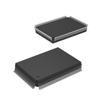
DF2367VF33 Renesas Electronics America, DF2367VF33 Datasheet - Page 794

DF2367VF33
Manufacturer Part Number
DF2367VF33
Description
MCU 3V 384K 128-QFP
Manufacturer
Renesas Electronics America
Series
H8® H8S/2300r
Datasheet
1.DF2368VTE34V.pdf
(1044 pages)
Specifications of DF2367VF33
Core Processor
H8S/2000
Core Size
16-Bit
Speed
33MHz
Connectivity
I²C, IrDA, SCI, SmartCard
Peripherals
DMA, POR, PWM, WDT
Number Of I /o
84
Program Memory Size
384KB (384K x 8)
Program Memory Type
FLASH
Ram Size
24K x 8
Voltage - Supply (vcc/vdd)
3 V ~ 3.6 V
Data Converters
A/D 10x10b, D/A 2x8b
Oscillator Type
Internal
Operating Temperature
-20°C ~ 75°C
Package / Case
128-QFP
Lead Free Status / RoHS Status
Contains lead / RoHS non-compliant
Eeprom Size
-
Other names
HD64F2367VF33
HD64F2367VF33
HD64F2367VF33
Available stocks
Company
Part Number
Manufacturer
Quantity
Price
Company:
Part Number:
DF2367VF33V
Manufacturer:
Renesas Electronics America
Quantity:
135
Company:
Part Number:
DF2367VF33V
Manufacturer:
Renesas Electronics America
Quantity:
10 000
Company:
Part Number:
DF2367VF33WV
Manufacturer:
Renesas Electronics America
Quantity:
10 000
- Current page: 794 of 1044
- Download datasheet (6Mb)
Section 20 Flash Memory (0.18-μm F-ZTAT Version)
• Flash Transfer Destination Address Register (FTDAR)
Bit
7
6
5
4
3
2
1
0
Rev.6.00 Mar. 18, 2009 Page 734 of 980
REJ09B0050-0600
FTDAR is a register that specify the address to download an on-chip program. This register
must be specified before setting the SCO bit in FCCS to 1.
Bit
Name
TDER
TDA6
TDA5
TDA4
TDA3
TDA2
TDA1
TDA0
Initial
Value
0
0
0
0
0
0
0
0
R/W
R/W
R/W
R/W
R/W
R/W
R/W
R/W
R/W
Description
Transfer Destination Address Setting Error
This bit is set to 1 when the address specified by bits
TDA6 to TDA0, which is the start address to download an
on-chip program, is over the range. Whether or not the
range specified by bits TDA6 to TDA0 is within the range
of H'00 to H'03 is determined when an on-chip program is
downloaded by setting the SCO bit in FCCS. Make sure
that this bit is cleared to 0 before setting the SCO bit to 1
and the value specified by TDA6 to TDA0 is within the
range of H'00 to H'03.
0: The value specified by bits TDA6 to TDA0 is within the
1: The value specified by is TDA6 to TDA0 is over the
Transfer Destination Address
Specifies the start address to download an on-chip
program. H'00 to H'03 can be specified meaning that the
start address in the on-chip RAM space can be specified
in units of 4 kbytes.
H'00: H'FF9000 is specified as a start address to
H'01: H'FFA000 is specified as a start address to
H'02: H'FFB000 is specified as a start address to
H'03: H'FF8000 is specified as a start address to
H'04 to H'07: Setting prohibited. Specifying this value
range.
range (H'04 to H'FF) and the download is stopped.
download an on-chip program.
download an on-chip program.
download an on-chip program.
download an on-chip program.
sets the TDRE bit to 1 and stops the
download.
Related parts for DF2367VF33
Image
Part Number
Description
Manufacturer
Datasheet
Request
R

Part Number:
Description:
CONN PLUG 12POS DUAL 0.5MM SMD
Manufacturer:
Hirose Electric Co Ltd
Datasheet:

Part Number:
Description:
CONN PLUG 18POS DUAL 0.5MM SMD
Manufacturer:
Hirose Electric Co Ltd
Datasheet:

Part Number:
Description:
CONN PLUG 14POS DUAL 0.5MM SMD
Manufacturer:
Hirose Electric Co Ltd
Datasheet:

Part Number:
Description:
CONN RECEPT 20POS DUAL 0.5MM SMD
Manufacturer:
Hirose Electric Co Ltd
Datasheet:

Part Number:
Description:
CONN PLUG 16POS DUAL 0.5MM SMD
Manufacturer:
Hirose Electric Co Ltd
Datasheet:

Part Number:
Description:
CONN RECEPT 16POS DUAL 0.5MM SMD
Manufacturer:
Hirose Electric Co Ltd
Datasheet:

Part Number:
Description:
CONN PLUG 20POS DUAL 0.5MM SMD
Manufacturer:
Hirose Electric Co Ltd
Datasheet:

Part Number:
Description:
CONN PLUG 30POS DUAL 0.5MM SMD
Manufacturer:
Hirose Electric Co Ltd
Datasheet:

Part Number:
Description:
CONN RECEPT 30POS DUAL 0.5MM SMD
Manufacturer:
Hirose Electric Co Ltd
Datasheet:

Part Number:
Description:
CONN PLUG 40POS DUAL 0.5MM SMD
Manufacturer:
Hirose Electric Co Ltd
Datasheet:

Part Number:
Description:
KIT STARTER FOR M16C/29
Manufacturer:
Renesas Electronics America
Datasheet:

Part Number:
Description:
KIT STARTER FOR R8C/2D
Manufacturer:
Renesas Electronics America
Datasheet:

Part Number:
Description:
R0K33062P STARTER KIT
Manufacturer:
Renesas Electronics America
Datasheet:

Part Number:
Description:
KIT STARTER FOR R8C/23 E8A
Manufacturer:
Renesas Electronics America
Datasheet:

Part Number:
Description:
KIT STARTER FOR R8C/25
Manufacturer:
Renesas Electronics America
Datasheet:


