MC908LJ12CFUE Freescale Semiconductor, MC908LJ12CFUE Datasheet - Page 133
MC908LJ12CFUE
Manufacturer Part Number
MC908LJ12CFUE
Description
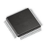
IC MCU 12K FLASH 4/8MHZ 64-QFP
Manufacturer
Freescale Semiconductor
Series
HC08r
Datasheet
1.MC68HC98LJ12CFUE.pdf
(414 pages)
Specifications of MC908LJ12CFUE
Core Processor
HC08
Core Size
8-Bit
Speed
8MHz
Connectivity
IRSCI, SPI
Peripherals
LCD, LVD, POR, PWM
Number Of I /o
32
Program Memory Size
12KB (12K x 8)
Program Memory Type
FLASH
Ram Size
512 x 8
Voltage - Supply (vcc/vdd)
3 V ~ 5.5 V
Data Converters
A/D 6x10b
Oscillator Type
Internal
Operating Temperature
-40°C ~ 85°C
Package / Case
64-QFP
Processor Series
HC08LJ
Core
HC08
Data Bus Width
8 bit
Data Ram Size
512 B
Interface Type
SCI, SPI
Maximum Clock Frequency
8 MHz
Number Of Programmable I/os
32
Number Of Timers
4
Maximum Operating Temperature
+ 85 C
Mounting Style
SMD/SMT
Development Tools By Supplier
FSICEBASE, M68EML08LJLKE, ZK-HC08LX-A, M68CBL05CE
Minimum Operating Temperature
- 40 C
On-chip Adc
10 bit, 6 Channel
Lead Free Status / RoHS Status
Lead free / RoHS Compliant
Eeprom Size
-
Lead Free Status / Rohs Status
Details
Available stocks
Company
Part Number
Manufacturer
Quantity
Price

Company:
Part Number:
MC908LJ12CFUE
Manufacturer:
Freescale Semiconductor
Quantity:
10 000
Company:
Part Number:
MC908LJ12CFUER
Manufacturer:
Freescale Semiconductor
Quantity:
10 000


MC68HC908LJ12
Freescale Semiconductor
PIN LOGIC
RESET
Signal Name
CGMXCLK
CGMPCLK
CGMOUT
PORRST
ICLK
IRST
R/W
IAB
IDB
—
V
DD
Rev. 2.1
INTERNAL
PULLUP
DEVICE
SIM RESET STATUS REGISTER
Internal RC oscillator clock
Buffered version of OSC1 from the oscillator module
PLL output and the divided PLL output
PLL-based or oscillator-based clock output from CGM module
(Bus clock = CGMOUT ÷ 2)
Internal address bus
Internal data bus
Signal from the power-on reset module to the SIM
Internal reset signal
Read/write signal
RESET PIN CONTROL
Table 9-1. Signal Name Conventions
POR CONTROL
AND PRIORITY DECODE
STOP/WAIT
INTERRUPT CONTROL
CONTROL
CONTROL
Figure 9-1. SIM Block Diagram
CLOCK
System Integration Module (SIM)
CLOCK GENERATORS
RESET
COUNTER
SIM
÷ 2
CONTROL
MASTER
RESET
Description
MODULE STOP
MODULE WAIT
CPU STOP (FROM CPU)
CPU WAIT (FROM CPU)
SIMOSCEN (TO CGM, OSC)
COP CLOCK
ICLK (FROM OSC)
CGMOUT (FROM CGM)
INTERNAL CLOCKS
LVI (FROM LVI MODULE)
ILLEGAL OPCODE (FROM CPU)
ILLEGAL ADDRESS (FROM ADDRESS
MAP DECODERS)
COP (FROM COP MODULE)
CPU INTERFACE
INTERRUPT SOURCES
System Integration Module (SIM)
Technical Data
133
Related parts for MC908LJ12CFUE
Image
Part Number
Description
Manufacturer
Datasheet
Request
R

Part Number:
Description:
Manufacturer:
Freescale Semiconductor, Inc
Datasheet:
Part Number:
Description:
Manufacturer:
Freescale Semiconductor, Inc
Datasheet:
Part Number:
Description:
Manufacturer:
Freescale Semiconductor, Inc
Datasheet:
Part Number:
Description:
Manufacturer:
Freescale Semiconductor, Inc
Datasheet:
Part Number:
Description:
Manufacturer:
Freescale Semiconductor, Inc
Datasheet:
Part Number:
Description:
Manufacturer:
Freescale Semiconductor, Inc
Datasheet:
Part Number:
Description:
Manufacturer:
Freescale Semiconductor, Inc
Datasheet:
Part Number:
Description:
Manufacturer:
Freescale Semiconductor, Inc
Datasheet:
Part Number:
Description:
Manufacturer:
Freescale Semiconductor, Inc
Datasheet:
Part Number:
Description:
Manufacturer:
Freescale Semiconductor, Inc
Datasheet:
Part Number:
Description:
Manufacturer:
Freescale Semiconductor, Inc
Datasheet:
Part Number:
Description:
Manufacturer:
Freescale Semiconductor, Inc
Datasheet:
Part Number:
Description:
Manufacturer:
Freescale Semiconductor, Inc
Datasheet:
Part Number:
Description:
Manufacturer:
Freescale Semiconductor, Inc
Datasheet:
Part Number:
Description:
Manufacturer:
Freescale Semiconductor, Inc
Datasheet: