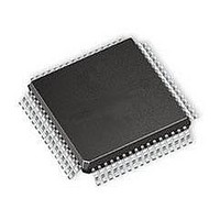
MC908LJ12CFUE Freescale Semiconductor, MC908LJ12CFUE Datasheet - Page 323

MC908LJ12CFUE
Manufacturer Part Number
MC908LJ12CFUE
Description
IC MCU 12K FLASH 4/8MHZ 64-QFP
Manufacturer
Freescale Semiconductor
Series
HC08r
Datasheet
1.MC68HC98LJ12CFUE.pdf
(414 pages)
Specifications of MC908LJ12CFUE
Core Processor
HC08
Core Size
8-Bit
Speed
8MHz
Connectivity
IRSCI, SPI
Peripherals
LCD, LVD, POR, PWM
Number Of I /o
32
Program Memory Size
12KB (12K x 8)
Program Memory Type
FLASH
Ram Size
512 x 8
Voltage - Supply (vcc/vdd)
3 V ~ 5.5 V
Data Converters
A/D 6x10b
Oscillator Type
Internal
Operating Temperature
-40°C ~ 85°C
Package / Case
64-QFP
Processor Series
HC08LJ
Core
HC08
Data Bus Width
8 bit
Data Ram Size
512 B
Interface Type
SCI, SPI
Maximum Clock Frequency
8 MHz
Number Of Programmable I/os
32
Number Of Timers
4
Maximum Operating Temperature
+ 85 C
Mounting Style
SMD/SMT
Development Tools By Supplier
FSICEBASE, M68EML08LJLKE, ZK-HC08LX-A, M68CBL05CE
Minimum Operating Temperature
- 40 C
On-chip Adc
10 bit, 6 Channel
Lead Free Status / RoHS Status
Lead free / RoHS Compliant
Eeprom Size
-
Lead Free Status / Rohs Status
Details
Available stocks
Company
Part Number
Manufacturer
Quantity
Price
Company:
Part Number:
MC908LJ12CFUE
Manufacturer:
Freescale Semiconductor
Quantity:
10 000
Company:
Part Number:
MC908LJ12CFUER
Manufacturer:
Freescale Semiconductor
Quantity:
10 000
- Current page: 323 of 414
- Download datasheet (5Mb)
16.5.2 LCD Voltages (V
16.5.3 LCD Cycle Frame
MC68HC908LJ12
Freescale Semiconductor
—
Rev. 2.1
The voltage V
are internal bias voltages for the LCD driver waveforms. They are
derived from V
The relative potential of the LCD voltages are:
The V
bits, LCCON[2:0].
The LCD driver module uses the CGMXCLK (see
(OSC)) as the input reference clock. This clock is divided to produce the
LCD waveform base clock, LCDCLK, by configuring the LCLK[2:0] bits
in the LCD clock register. The LCDCLK clocks the backplane and the
frontplane output waveforms.
The LCD cycle frame is determined by the equation:
For example, for 1/3 duty and 256Hz waveform base clock:
LCD,
•
•
•
•
LCD3
V
V
V
V
V
LCD CYCLE FRAME =
LCD1,
LCD
LCD1
LCD2
LCD3
LCD CYCLE FRAME =
Liquid Crystal Display Driver (LCD)
bias voltage, V
= V
= 2/3 × (V
= 1/3 × (V
= V
V
LCD
LCD2
LCD
DD
bias
is connected directly to V
using a resistor ladder (see
, V
LCD3
LCD
LCD
bias
= 11.72 ms
)
– V
– V
LCD WAVEFORM BASE CLOCK × DUTY
256 × (1/3)
, is controlled by the LCD contrast control
bias
bias
1
)
)
Liquid Crystal Display Driver (LCD)
DD
. V
1
Figure
LCD1
Section 7. Oscillator
, V
16-3).
LCD2
Technical Data
, and V
LCD3
323
Related parts for MC908LJ12CFUE
Image
Part Number
Description
Manufacturer
Datasheet
Request
R
Part Number:
Description:
Manufacturer:
Freescale Semiconductor, Inc
Datasheet:
Part Number:
Description:
Manufacturer:
Freescale Semiconductor, Inc
Datasheet:
Part Number:
Description:
Manufacturer:
Freescale Semiconductor, Inc
Datasheet:
Part Number:
Description:
Manufacturer:
Freescale Semiconductor, Inc
Datasheet:
Part Number:
Description:
Manufacturer:
Freescale Semiconductor, Inc
Datasheet:
Part Number:
Description:
Manufacturer:
Freescale Semiconductor, Inc
Datasheet:
Part Number:
Description:
Manufacturer:
Freescale Semiconductor, Inc
Datasheet:
Part Number:
Description:
Manufacturer:
Freescale Semiconductor, Inc
Datasheet:
Part Number:
Description:
Manufacturer:
Freescale Semiconductor, Inc
Datasheet:
Part Number:
Description:
Manufacturer:
Freescale Semiconductor, Inc
Datasheet:
Part Number:
Description:
Manufacturer:
Freescale Semiconductor, Inc
Datasheet:
Part Number:
Description:
Manufacturer:
Freescale Semiconductor, Inc
Datasheet:
Part Number:
Description:
Manufacturer:
Freescale Semiconductor, Inc
Datasheet:
Part Number:
Description:
Manufacturer:
Freescale Semiconductor, Inc
Datasheet:
Part Number:
Description:
Manufacturer:
Freescale Semiconductor, Inc
Datasheet:


