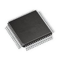
MC908LJ12CFUE Freescale Semiconductor, MC908LJ12CFUE Datasheet - Page 207

MC908LJ12CFUE
Manufacturer Part Number
MC908LJ12CFUE
Description
IC MCU 12K FLASH 4/8MHZ 64-QFP
Manufacturer
Freescale Semiconductor
Series
HC08r
Datasheet
1.MC68HC98LJ12CFUE.pdf
(414 pages)
Specifications of MC908LJ12CFUE
Core Processor
HC08
Core Size
8-Bit
Speed
8MHz
Connectivity
IRSCI, SPI
Peripherals
LCD, LVD, POR, PWM
Number Of I /o
32
Program Memory Size
12KB (12K x 8)
Program Memory Type
FLASH
Ram Size
512 x 8
Voltage - Supply (vcc/vdd)
3 V ~ 5.5 V
Data Converters
A/D 6x10b
Oscillator Type
Internal
Operating Temperature
-40°C ~ 85°C
Package / Case
64-QFP
Processor Series
HC08LJ
Core
HC08
Data Bus Width
8 bit
Data Ram Size
512 B
Interface Type
SCI, SPI
Maximum Clock Frequency
8 MHz
Number Of Programmable I/os
32
Number Of Timers
4
Maximum Operating Temperature
+ 85 C
Mounting Style
SMD/SMT
Development Tools By Supplier
FSICEBASE, M68EML08LJLKE, ZK-HC08LX-A, M68CBL05CE
Minimum Operating Temperature
- 40 C
On-chip Adc
10 bit, 6 Channel
Lead Free Status / RoHS Status
Lead free / RoHS Compliant
Eeprom Size
-
Lead Free Status / Rohs Status
Details
Available stocks
Company
Part Number
Manufacturer
Quantity
Price
Company:
Part Number:
MC908LJ12CFUE
Manufacturer:
Freescale Semiconductor
Quantity:
10 000
Company:
Part Number:
MC908LJ12CFUER
Manufacturer:
Freescale Semiconductor
Quantity:
10 000
- Current page: 207 of 414
- Download datasheet (5Mb)
11.10.5 TIM Channel Registers
MC68HC908LJ12
Freescale Semiconductor
NOTE:
NOTE:
—
Rev. 2.1
Before enabling a TIM channel register for input capture operation, make
sure that the TCHx pin is stable for at least two bus clocks. User software
should also clear CHxF before setting CHxIE to avoid any false
interrupts.
TOVx — Toggle On Overflow Bit
When TOVx is set, a TIM counter overflow takes precedence over a
channel x output compare if both occur at the same time.
CHxMAX — Channel x Maximum Duty Cycle Bit
These read/write registers contain the captured TIM counter value of the
input capture function or the output compare value of the output
compare function. The state of the TIM channel registers after reset is
unknown.
CHxMAX
TCHx
When channel x is an output compare channel, this read/write bit
controls the behavior of the channel x output when the TIM counter
overflows. When channel x is an input capture channel, TOVx has no
effect. Reset clears the TOVx bit.
When the TOVx bit is at logic 1, setting the CHxMAX bit forces the
duty cycle of buffered and unbuffered PWM signals to 100%. As
Figure 11-11
is set or cleared. The output stays at the 100% duty cycle level until
the cycle after CHxMAX is cleared.
1 = Channel x pin toggles on TIM counter overflow
0 = Channel x pin does not toggle on TIM counter overflow
OVERFLOW
Timer Interface Module (TIM)
COMPARE
PERIOD
OUTPUT
shows, the CHxMAX bit takes effect in the cycle after it
Figure 11-11. CHxMAX Latency
OVERFLOW
COMPARE
OUTPUT
OVERFLOW
COMPARE
OUTPUT
OVERFLOW
Timer Interface Module (TIM)
COMPARE
OUTPUT
OVERFLOW
Technical Data
207
Related parts for MC908LJ12CFUE
Image
Part Number
Description
Manufacturer
Datasheet
Request
R
Part Number:
Description:
Manufacturer:
Freescale Semiconductor, Inc
Datasheet:
Part Number:
Description:
Manufacturer:
Freescale Semiconductor, Inc
Datasheet:
Part Number:
Description:
Manufacturer:
Freescale Semiconductor, Inc
Datasheet:
Part Number:
Description:
Manufacturer:
Freescale Semiconductor, Inc
Datasheet:
Part Number:
Description:
Manufacturer:
Freescale Semiconductor, Inc
Datasheet:
Part Number:
Description:
Manufacturer:
Freescale Semiconductor, Inc
Datasheet:
Part Number:
Description:
Manufacturer:
Freescale Semiconductor, Inc
Datasheet:
Part Number:
Description:
Manufacturer:
Freescale Semiconductor, Inc
Datasheet:
Part Number:
Description:
Manufacturer:
Freescale Semiconductor, Inc
Datasheet:
Part Number:
Description:
Manufacturer:
Freescale Semiconductor, Inc
Datasheet:
Part Number:
Description:
Manufacturer:
Freescale Semiconductor, Inc
Datasheet:
Part Number:
Description:
Manufacturer:
Freescale Semiconductor, Inc
Datasheet:
Part Number:
Description:
Manufacturer:
Freescale Semiconductor, Inc
Datasheet:
Part Number:
Description:
Manufacturer:
Freescale Semiconductor, Inc
Datasheet:
Part Number:
Description:
Manufacturer:
Freescale Semiconductor, Inc
Datasheet:


