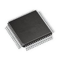
MC908LJ12CFUE Freescale Semiconductor, MC908LJ12CFUE Datasheet - Page 187

MC908LJ12CFUE
Manufacturer Part Number
MC908LJ12CFUE
Description
IC MCU 12K FLASH 4/8MHZ 64-QFP
Manufacturer
Freescale Semiconductor
Series
HC08r
Datasheet
1.MC68HC98LJ12CFUE.pdf
(414 pages)
Specifications of MC908LJ12CFUE
Core Processor
HC08
Core Size
8-Bit
Speed
8MHz
Connectivity
IRSCI, SPI
Peripherals
LCD, LVD, POR, PWM
Number Of I /o
32
Program Memory Size
12KB (12K x 8)
Program Memory Type
FLASH
Ram Size
512 x 8
Voltage - Supply (vcc/vdd)
3 V ~ 5.5 V
Data Converters
A/D 6x10b
Oscillator Type
Internal
Operating Temperature
-40°C ~ 85°C
Package / Case
64-QFP
Processor Series
HC08LJ
Core
HC08
Data Bus Width
8 bit
Data Ram Size
512 B
Interface Type
SCI, SPI
Maximum Clock Frequency
8 MHz
Number Of Programmable I/os
32
Number Of Timers
4
Maximum Operating Temperature
+ 85 C
Mounting Style
SMD/SMT
Development Tools By Supplier
FSICEBASE, M68EML08LJLKE, ZK-HC08LX-A, M68CBL05CE
Minimum Operating Temperature
- 40 C
On-chip Adc
10 bit, 6 Channel
Lead Free Status / RoHS Status
Lead free / RoHS Compliant
Eeprom Size
-
Lead Free Status / Rohs Status
Details
Available stocks
Company
Part Number
Manufacturer
Quantity
Price
Company:
Part Number:
MC908LJ12CFUE
Manufacturer:
Freescale Semiconductor
Quantity:
10 000
Company:
Part Number:
MC908LJ12CFUER
Manufacturer:
Freescale Semiconductor
Quantity:
10 000
- Current page: 187 of 414
- Download datasheet (5Mb)
11.4 Pin Name Conventions
11.5 Functional Description
MC68HC908LJ12
Freescale Semiconductor
NOTE:
—
Rev. 2.1
The text that follows describes both timers, TIM1 and TIM2. The TIM
input/output (I/O) pin names are T[1,2]CH0 (timer channel 0) and
T[1,2]CH1 (timer channel 1), where “1” is used to indicate TIM1 and “2”
is used to indicate TIM2. The two TIMs share four I/O pins with four I/O
port pins. The full names of the TIM I/O pins are listed in
Table
References to either timer 1 or timer 2 may be made in the following text
by omitting the timer number. For example, TCH0 may refer generically
to T1CH0 and T2CH0, and TCH1 may refer to T1CH1 and T2CH1.
Figure 11-1
the TIM is the 16-bit TIM counter that can operate as a free-running
counter or a modulo up-counter. The TIM counter provides the timing
reference for the input capture and output compare functions. The TIM
counter modulo registers, TMODH:TMODL, control the modulo value of
the TIM counter. Software can read the TIM counter value at any time
without affecting the counting sequence.
The two TIM channels (per timer) are programmable independently as
input capture or output compare channels.
Pin Names:
TIM Generic Pin Names:
Full TIM
11-1. The generic pin names appear in the text that follows.
Timer Interface Module (TIM)
shows the structure of the TIM. The central component of
Table 11-1. Pin Name Conventions
TIM1
TIM2
PTB2/T1CH0
PTB4/T2CH0
T[1,2]CH0
Timer Interface Module (TIM)
PTB3/T1CH1
PTB5/T2CH1
T[1,2]CH1
Technical Data
187
Related parts for MC908LJ12CFUE
Image
Part Number
Description
Manufacturer
Datasheet
Request
R
Part Number:
Description:
Manufacturer:
Freescale Semiconductor, Inc
Datasheet:
Part Number:
Description:
Manufacturer:
Freescale Semiconductor, Inc
Datasheet:
Part Number:
Description:
Manufacturer:
Freescale Semiconductor, Inc
Datasheet:
Part Number:
Description:
Manufacturer:
Freescale Semiconductor, Inc
Datasheet:
Part Number:
Description:
Manufacturer:
Freescale Semiconductor, Inc
Datasheet:
Part Number:
Description:
Manufacturer:
Freescale Semiconductor, Inc
Datasheet:
Part Number:
Description:
Manufacturer:
Freescale Semiconductor, Inc
Datasheet:
Part Number:
Description:
Manufacturer:
Freescale Semiconductor, Inc
Datasheet:
Part Number:
Description:
Manufacturer:
Freescale Semiconductor, Inc
Datasheet:
Part Number:
Description:
Manufacturer:
Freescale Semiconductor, Inc
Datasheet:
Part Number:
Description:
Manufacturer:
Freescale Semiconductor, Inc
Datasheet:
Part Number:
Description:
Manufacturer:
Freescale Semiconductor, Inc
Datasheet:
Part Number:
Description:
Manufacturer:
Freescale Semiconductor, Inc
Datasheet:
Part Number:
Description:
Manufacturer:
Freescale Semiconductor, Inc
Datasheet:
Part Number:
Description:
Manufacturer:
Freescale Semiconductor, Inc
Datasheet:


