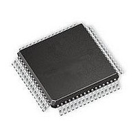
MC908LJ12CFUE Freescale Semiconductor, MC908LJ12CFUE Datasheet - Page 72

MC908LJ12CFUE
Manufacturer Part Number
MC908LJ12CFUE
Description
IC MCU 12K FLASH 4/8MHZ 64-QFP
Manufacturer
Freescale Semiconductor
Series
HC08r
Datasheet
1.MC68HC98LJ12CFUE.pdf
(414 pages)
Specifications of MC908LJ12CFUE
Core Processor
HC08
Core Size
8-Bit
Speed
8MHz
Connectivity
IRSCI, SPI
Peripherals
LCD, LVD, POR, PWM
Number Of I /o
32
Program Memory Size
12KB (12K x 8)
Program Memory Type
FLASH
Ram Size
512 x 8
Voltage - Supply (vcc/vdd)
3 V ~ 5.5 V
Data Converters
A/D 6x10b
Oscillator Type
Internal
Operating Temperature
-40°C ~ 85°C
Package / Case
64-QFP
Processor Series
HC08LJ
Core
HC08
Data Bus Width
8 bit
Data Ram Size
512 B
Interface Type
SCI, SPI
Maximum Clock Frequency
8 MHz
Number Of Programmable I/os
32
Number Of Timers
4
Maximum Operating Temperature
+ 85 C
Mounting Style
SMD/SMT
Development Tools By Supplier
FSICEBASE, M68EML08LJLKE, ZK-HC08LX-A, M68CBL05CE
Minimum Operating Temperature
- 40 C
On-chip Adc
10 bit, 6 Channel
Lead Free Status / RoHS Status
Lead free / RoHS Compliant
Eeprom Size
-
Lead Free Status / Rohs Status
Details
Available stocks
Company
Part Number
Manufacturer
Quantity
Price
Company:
Part Number:
MC908LJ12CFUE
Manufacturer:
Freescale Semiconductor
Quantity:
10 000
Company:
Part Number:
MC908LJ12CFUER
Manufacturer:
Freescale Semiconductor
Quantity:
10 000
- Current page: 72 of 414
- Download datasheet (5Mb)
Configuration Registers (CONFIG)
5.3 Functional Description
Technical Data
72
† One-time writable register after each reset.
†† Reset by POR only.
$001D
Addr.
$001F
Configuration Register 2
Configuration Register 1
Register Name
NOTE:
(CONFIG2)
(CONFIG1)
†
†
The configuration registers are used in the initialization of various
options. The configuration registers can be written once after each reset.
All of the configuration register bits are cleared during reset. Since the
various options affect the operation of the MCU, it is recommended that
these registers be written immediately after reset. The configuration
registers are located at $001D and $001F. The configuration registers
may be read at anytime.
The options except LVISEL[1:0] are one-time writable by the user after
each reset. The LVISEL[1:0] bits are one-time writable by the user only
after each POR (power-on reset). The CONFIG registers are not in the
FLASH memory but are special registers containing one-time writable
latches after each reset. Upon a reset, the CONFIG registers default to
predetermined settings as shown in
Reset:
Reset:
Read:
Read:
Write:
Write:
Figure 5-1. CONFIG Registers Summary
COPRS
Bit 7
Configuration Registers (CONFIG)
0
0
0
LVISTOP LVIRSTD LVIPWRD
= Unimplemented
IRCDIS
STOP_
6
0
0
XCLKEN
STOP_
5
0
0
DIV2CLK
4
0
1
Figure 5-2
PCEH
3
0
0
0
MC68HC908LJ12
and
SSREC
PCEL
Freescale Semiconductor
0
0
2
Figure
LVISEL1
STOP
0
1
0
††
5-3.
—
LVISEL0
Rev. 2.1
COPD
Bit 0
0
0
††
Related parts for MC908LJ12CFUE
Image
Part Number
Description
Manufacturer
Datasheet
Request
R
Part Number:
Description:
Manufacturer:
Freescale Semiconductor, Inc
Datasheet:
Part Number:
Description:
Manufacturer:
Freescale Semiconductor, Inc
Datasheet:
Part Number:
Description:
Manufacturer:
Freescale Semiconductor, Inc
Datasheet:
Part Number:
Description:
Manufacturer:
Freescale Semiconductor, Inc
Datasheet:
Part Number:
Description:
Manufacturer:
Freescale Semiconductor, Inc
Datasheet:
Part Number:
Description:
Manufacturer:
Freescale Semiconductor, Inc
Datasheet:
Part Number:
Description:
Manufacturer:
Freescale Semiconductor, Inc
Datasheet:
Part Number:
Description:
Manufacturer:
Freescale Semiconductor, Inc
Datasheet:
Part Number:
Description:
Manufacturer:
Freescale Semiconductor, Inc
Datasheet:
Part Number:
Description:
Manufacturer:
Freescale Semiconductor, Inc
Datasheet:
Part Number:
Description:
Manufacturer:
Freescale Semiconductor, Inc
Datasheet:
Part Number:
Description:
Manufacturer:
Freescale Semiconductor, Inc
Datasheet:
Part Number:
Description:
Manufacturer:
Freescale Semiconductor, Inc
Datasheet:
Part Number:
Description:
Manufacturer:
Freescale Semiconductor, Inc
Datasheet:
Part Number:
Description:
Manufacturer:
Freescale Semiconductor, Inc
Datasheet:


