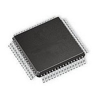
MC908LJ12CFUE Freescale Semiconductor, MC908LJ12CFUE Datasheet - Page 303

MC908LJ12CFUE
Manufacturer Part Number
MC908LJ12CFUE
Description
IC MCU 12K FLASH 4/8MHZ 64-QFP
Manufacturer
Freescale Semiconductor
Series
HC08r
Datasheet
1.MC68HC98LJ12CFUE.pdf
(414 pages)
Specifications of MC908LJ12CFUE
Core Processor
HC08
Core Size
8-Bit
Speed
8MHz
Connectivity
IRSCI, SPI
Peripherals
LCD, LVD, POR, PWM
Number Of I /o
32
Program Memory Size
12KB (12K x 8)
Program Memory Type
FLASH
Ram Size
512 x 8
Voltage - Supply (vcc/vdd)
3 V ~ 5.5 V
Data Converters
A/D 6x10b
Oscillator Type
Internal
Operating Temperature
-40°C ~ 85°C
Package / Case
64-QFP
Processor Series
HC08LJ
Core
HC08
Data Bus Width
8 bit
Data Ram Size
512 B
Interface Type
SCI, SPI
Maximum Clock Frequency
8 MHz
Number Of Programmable I/os
32
Number Of Timers
4
Maximum Operating Temperature
+ 85 C
Mounting Style
SMD/SMT
Development Tools By Supplier
FSICEBASE, M68EML08LJLKE, ZK-HC08LX-A, M68CBL05CE
Minimum Operating Temperature
- 40 C
On-chip Adc
10 bit, 6 Channel
Lead Free Status / RoHS Status
Lead free / RoHS Compliant
Eeprom Size
-
Lead Free Status / Rohs Status
Details
Available stocks
Company
Part Number
Manufacturer
Quantity
Price
Company:
Part Number:
MC908LJ12CFUE
Manufacturer:
Freescale Semiconductor
Quantity:
10 000
Company:
Part Number:
MC908LJ12CFUER
Manufacturer:
Freescale Semiconductor
Quantity:
10 000
- Current page: 303 of 414
- Download datasheet (5Mb)
15.4 Functional Description
15.4.1 ADC Port I/O Pins
MC68HC908LJ12
Freescale Semiconductor
Addr.
$003C
$003D
$003E
$003F
ADC Data Register High
ADC Status and Control
ADC Data Register Low
Register Name
ADC Clock Register
—
Rev. 2.1
(ADSCR)
(ADCLK)
Register
(ADRH)
(ADRL)
The ADC provides six pins for sampling external sources at pins
PTA4/ADC0–PTA7/ADC3 and PTB6/ADC4–PTB7/ADC5. An analog
multiplexer allows the single ADC converter to select one of nine ADC
channels as ADC voltage in (V
successive approximation register-based analog-to-digital converter.
When the conversion is completed, ADC places the result in the ADC
data register, high and low byte (ADRH and ADRL), and sets a flag or
generates an interrupt.
Figure 15-2
PTA4–PTA7 and PTB6–PTB7 are general-purpose I/O pins that are
shared with the ADC channels. The channel select bits, ADCH[4:0],
define which ADC channel/port pin will be used as the input signal. The
ADC overrides the port I/O logic by forcing that pin as input to the ADC.
The remaining ADC channels/port pins are controlled by the port I/O
Reset:
Reset:
Reset:
Reset:
Read:
Read:
Read:
Read:
Write:
Write:
Write:
Write:
Figure 15-1. ADC I/O Register Summary
COCO
ADIV2
Bit 7
ADx
ADx
Analog-to-Digital Converter (ADC)
R
R
0
0
0
0
shows the structure of the ADC module.
= Unimplemented
ADIV1
AIEN
ADx
ADx
R
R
6
0
0
0
0
ADCO
ADIV0
ADx
ADx
R
R
5
0
0
0
0
ADIN
ADICLK
ADCH4
ADx
ADx
R
R
4
1
0
0
0
). V
ADIN
MODE1
ADCH3
ADx
ADx
R
R
R
3
1
0
0
0
Analog-to-Digital Converter (ADC)
is converted by the
= Reserved
MODE0
ADCH2
ADx
ADx
R
R
2
1
0
0
1
ADCH1
ADx
ADx
R
R
1
1
0
0
0
0
Technical Data
ADCH0
Bit 0
ADx
ADx
R
R
R
1
0
0
0
0
303
Related parts for MC908LJ12CFUE
Image
Part Number
Description
Manufacturer
Datasheet
Request
R
Part Number:
Description:
Manufacturer:
Freescale Semiconductor, Inc
Datasheet:
Part Number:
Description:
Manufacturer:
Freescale Semiconductor, Inc
Datasheet:
Part Number:
Description:
Manufacturer:
Freescale Semiconductor, Inc
Datasheet:
Part Number:
Description:
Manufacturer:
Freescale Semiconductor, Inc
Datasheet:
Part Number:
Description:
Manufacturer:
Freescale Semiconductor, Inc
Datasheet:
Part Number:
Description:
Manufacturer:
Freescale Semiconductor, Inc
Datasheet:
Part Number:
Description:
Manufacturer:
Freescale Semiconductor, Inc
Datasheet:
Part Number:
Description:
Manufacturer:
Freescale Semiconductor, Inc
Datasheet:
Part Number:
Description:
Manufacturer:
Freescale Semiconductor, Inc
Datasheet:
Part Number:
Description:
Manufacturer:
Freescale Semiconductor, Inc
Datasheet:
Part Number:
Description:
Manufacturer:
Freescale Semiconductor, Inc
Datasheet:
Part Number:
Description:
Manufacturer:
Freescale Semiconductor, Inc
Datasheet:
Part Number:
Description:
Manufacturer:
Freescale Semiconductor, Inc
Datasheet:
Part Number:
Description:
Manufacturer:
Freescale Semiconductor, Inc
Datasheet:
Part Number:
Description:
Manufacturer:
Freescale Semiconductor, Inc
Datasheet:


