MC908LJ12CFUE Freescale Semiconductor, MC908LJ12CFUE Datasheet - Page 27
MC908LJ12CFUE
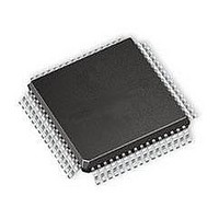
Manufacturer Part Number
MC908LJ12CFUE
Description
IC MCU 12K FLASH 4/8MHZ 64-QFP
Manufacturer
Freescale Semiconductor
Series
HC08r
Datasheet
1.MC68HC98LJ12CFUE.pdf
(414 pages)
Specifications of MC908LJ12CFUE
Core Processor
HC08
Core Size
8-Bit
Speed
8MHz
Connectivity
IRSCI, SPI
Peripherals
LCD, LVD, POR, PWM
Number Of I /o
32
Program Memory Size
12KB (12K x 8)
Program Memory Type
FLASH
Ram Size
512 x 8
Voltage - Supply (vcc/vdd)
3 V ~ 5.5 V
Data Converters
A/D 6x10b
Oscillator Type
Internal
Operating Temperature
-40°C ~ 85°C
Package / Case
64-QFP
Processor Series
HC08LJ
Core
HC08
Data Bus Width
8 bit
Data Ram Size
512 B
Interface Type
SCI, SPI
Maximum Clock Frequency
8 MHz
Number Of Programmable I/os
32
Number Of Timers
4
Maximum Operating Temperature
+ 85 C
Mounting Style
SMD/SMT
Development Tools By Supplier
FSICEBASE, M68EML08LJLKE, ZK-HC08LX-A, M68CBL05CE
Minimum Operating Temperature
- 40 C
On-chip Adc
10 bit, 6 Channel
Lead Free Status / RoHS Status
Lead free / RoHS Compliant
Eeprom Size
-
Lead Free Status / Rohs Status
Details
Available stocks
Company
Part Number
Manufacturer
Quantity
Price

Company:
Part Number:
MC908LJ12CFUE
Manufacturer:
Freescale Semiconductor
Quantity:
10 000
Company:
Part Number:
MC908LJ12CFUER
Manufacturer:
Freescale Semiconductor
Quantity:
10 000


MC68HC908LJ12
Freescale Semiconductor
—
Rev. 2.1
Figure
15-1 ADC I/O Register Summary . . . . . . . . . . . . . . . . . . . . . . . . . . 303
15-2 ADC Block Diagram . . . . . . . . . . . . . . . . . . . . . . . . . . . . . . . . 304
15-3 8-Bit Truncation Mode Error . . . . . . . . . . . . . . . . . . . . . . . . . . 307
15-4 ADC Status and Control Register (ADSCR) . . . . . . . . . . . . . . 310
15-5 ADRH and ADRL in 8-Bit Truncated Mode. . . . . . . . . . . . . . . 312
15-6 ADRH and ADRL in Right Justified Mode. . . . . . . . . . . . . . . . 312
15-7 ADRH and ADRL in Left Justified Mode . . . . . . . . . . . . . . . . . 313
15-8 ADRH and ADRL in Left Justified Sign Data Mode . . . . . . . . 313
15-9 ADC Clock Control Register (ADICLK). . . . . . . . . . . . . . . . . . 314
16-1 LCD I/O Register Summary . . . . . . . . . . . . . . . . . . . . . . . . . . 319
16-2 LCD Block Diagram . . . . . . . . . . . . . . . . . . . . . . . . . . . . . . . . 321
16-3 Simplified LCD Schematic (1/3 Duty, 1/3 Bias) . . . . . . . . . . . 322
16-4 Fast Charge Timing . . . . . . . . . . . . . . . . . . . . . . . . . . . . . . . . 324
16-5 1/3 Duty LCD Backplane Driver Waveforms. . . . . . . . . . . . . . 326
16-6 Static LCD Backplane Driver Waveform. . . . . . . . . . . . . . . . . 327
16-7 1/4 Duty LCD Backplane Driver Waveforms. . . . . . . . . . . . . . 327
16-8 Static LCD Frontplane Driver Waveforms. . . . . . . . . . . . . . . . 328
16-9 1/3 Duty LCD Frontplane Driver Waveforms . . . . . . . . . . . . . 329
16-10 1/4 Duty LCD Frontplane Driver Waveforms . . . . . . . . . . . . . 330
16-11 1/4 Duty LCD Frontplane Driver Waveforms (continued) . . . . 331
16-12 7-Segment Display Example . . . . . . . . . . . . . . . . . . . . . . . . . 332
16-13 BP0–BP2 and FP0–FP2 Output Waveforms for
16-14 "f" Segment Voltage Waveform . . . . . . . . . . . . . . . . . . . . . . .334
16-15 "e" Segment Voltage Waveform . . . . . . . . . . . . . . . . . . . . . . . 334
16-16 LCD Control Register (LCDCR) . . . . . . . . . . . . . . . . . . . . . . .335
16-17 LCD Clock Register (LCDCLK). . . . . . . . . . . . . . . . . . . . . . . . 337
16-18 LCD Data Registers 1–14 (LDAT1–LDAT14) . . . . . . . . . . . . . 339
17-1 I/O Port Register Summary. . . . . . . . . . . . . . . . . . . . . . . . . . .342
17-2 Port A Data Register (PTA) . . . . . . . . . . . . . . . . . . . . . . . . . . 344
17-3 Data Direction Register A (DDRA) . . . . . . . . . . . . . . . . . . . . . 345
17-4 Port A I/O Circuit. . . . . . . . . . . . . . . . . . . . . . . . . . . . . . . . . . . 346
17-5 Port B Data Register (PTB) . . . . . . . . . . . . . . . . . . . . . . . . . . 347
17-6 Data Direction Register B (DDRB) . . . . . . . . . . . . . . . . . . . . . 349
17-7 Port B I/O Circuit. . . . . . . . . . . . . . . . . . . . . . . . . . . . . . . . . . . 349
7-Segment Display Example . . . . . . . . . . . . . . . . . . . . . . . 333
List of Figures
Title
Technical Data
List of Figures
Page
27
Related parts for MC908LJ12CFUE
Image
Part Number
Description
Manufacturer
Datasheet
Request
R

Part Number:
Description:
Manufacturer:
Freescale Semiconductor, Inc
Datasheet:
Part Number:
Description:
Manufacturer:
Freescale Semiconductor, Inc
Datasheet:
Part Number:
Description:
Manufacturer:
Freescale Semiconductor, Inc
Datasheet:
Part Number:
Description:
Manufacturer:
Freescale Semiconductor, Inc
Datasheet:
Part Number:
Description:
Manufacturer:
Freescale Semiconductor, Inc
Datasheet:
Part Number:
Description:
Manufacturer:
Freescale Semiconductor, Inc
Datasheet:
Part Number:
Description:
Manufacturer:
Freescale Semiconductor, Inc
Datasheet:
Part Number:
Description:
Manufacturer:
Freescale Semiconductor, Inc
Datasheet:
Part Number:
Description:
Manufacturer:
Freescale Semiconductor, Inc
Datasheet:
Part Number:
Description:
Manufacturer:
Freescale Semiconductor, Inc
Datasheet:
Part Number:
Description:
Manufacturer:
Freescale Semiconductor, Inc
Datasheet:
Part Number:
Description:
Manufacturer:
Freescale Semiconductor, Inc
Datasheet:
Part Number:
Description:
Manufacturer:
Freescale Semiconductor, Inc
Datasheet:
Part Number:
Description:
Manufacturer:
Freescale Semiconductor, Inc
Datasheet:
Part Number:
Description:
Manufacturer:
Freescale Semiconductor, Inc
Datasheet: