MC908LJ12CFUE Freescale Semiconductor, MC908LJ12CFUE Datasheet - Page 277
MC908LJ12CFUE
Manufacturer Part Number
MC908LJ12CFUE
Description
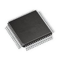
IC MCU 12K FLASH 4/8MHZ 64-QFP
Manufacturer
Freescale Semiconductor
Series
HC08r
Datasheet
1.MC68HC98LJ12CFUE.pdf
(414 pages)
Specifications of MC908LJ12CFUE
Core Processor
HC08
Core Size
8-Bit
Speed
8MHz
Connectivity
IRSCI, SPI
Peripherals
LCD, LVD, POR, PWM
Number Of I /o
32
Program Memory Size
12KB (12K x 8)
Program Memory Type
FLASH
Ram Size
512 x 8
Voltage - Supply (vcc/vdd)
3 V ~ 5.5 V
Data Converters
A/D 6x10b
Oscillator Type
Internal
Operating Temperature
-40°C ~ 85°C
Package / Case
64-QFP
Processor Series
HC08LJ
Core
HC08
Data Bus Width
8 bit
Data Ram Size
512 B
Interface Type
SCI, SPI
Maximum Clock Frequency
8 MHz
Number Of Programmable I/os
32
Number Of Timers
4
Maximum Operating Temperature
+ 85 C
Mounting Style
SMD/SMT
Development Tools By Supplier
FSICEBASE, M68EML08LJLKE, ZK-HC08LX-A, M68CBL05CE
Minimum Operating Temperature
- 40 C
On-chip Adc
10 bit, 6 Channel
Lead Free Status / RoHS Status
Lead free / RoHS Compliant
Eeprom Size
-
Lead Free Status / Rohs Status
Details
Available stocks
Company
Part Number
Manufacturer
Quantity
Price

Company:
Part Number:
MC908LJ12CFUE
Manufacturer:
Freescale Semiconductor
Quantity:
10 000
Company:
Part Number:
MC908LJ12CFUER
Manufacturer:
Freescale Semiconductor
Quantity:
10 000


MC68HC908LJ12
Freescale Semiconductor
CAPTURE STROBE
FOR REFERENCE
SPSCK; CPOL = 0
MASTER SS
SPSCK; CPOL =1
SPSCK CYCLE #
MISO/MOSI
FROM MASTER
SS; TO SLAVE
SLAVE SS
SLAVE SS
CPHA = 0
CPHA = 1
FROM SLAVE
—
Rev. 2.1
MOSI
MISO
Figure 14-4. Transmission Format (CPHA = 0)
When CPHA = 0 for a slave, the falling edge of SS indicates the
beginning of the transmission. This causes the SPI to leave its idle state
and begin driving the MISO pin with the MSB of its data. Once the
transmission begins, no new data is allowed into the shift register from
the transmit data register. Therefore, the SPI data register of the slave
must be loaded with transmit data before the falling edge of SS. Any data
written after the falling edge is stored in the transmit data register and
transferred to the shift register after the current transmission.
Serial Peripheral Interface Module (SPI)
MSB
Figure 14-5. CPHA/SS Timing
BYTE 1
MSB
1
BIT 6
BIT 6
2
BIT 5
BIT 5
3
BYTE 2
BIT 4
BIT 4
4
BIT 3
BIT 3
5
Serial Peripheral Interface Module (SPI)
BIT 2
BIT 2
6
BYTE 3
BIT 1
BIT 1
7
LSB
LSB
8
Technical Data
277
Related parts for MC908LJ12CFUE
Image
Part Number
Description
Manufacturer
Datasheet
Request
R

Part Number:
Description:
Manufacturer:
Freescale Semiconductor, Inc
Datasheet:
Part Number:
Description:
Manufacturer:
Freescale Semiconductor, Inc
Datasheet:
Part Number:
Description:
Manufacturer:
Freescale Semiconductor, Inc
Datasheet:
Part Number:
Description:
Manufacturer:
Freescale Semiconductor, Inc
Datasheet:
Part Number:
Description:
Manufacturer:
Freescale Semiconductor, Inc
Datasheet:
Part Number:
Description:
Manufacturer:
Freescale Semiconductor, Inc
Datasheet:
Part Number:
Description:
Manufacturer:
Freescale Semiconductor, Inc
Datasheet:
Part Number:
Description:
Manufacturer:
Freescale Semiconductor, Inc
Datasheet:
Part Number:
Description:
Manufacturer:
Freescale Semiconductor, Inc
Datasheet:
Part Number:
Description:
Manufacturer:
Freescale Semiconductor, Inc
Datasheet:
Part Number:
Description:
Manufacturer:
Freescale Semiconductor, Inc
Datasheet:
Part Number:
Description:
Manufacturer:
Freescale Semiconductor, Inc
Datasheet:
Part Number:
Description:
Manufacturer:
Freescale Semiconductor, Inc
Datasheet:
Part Number:
Description:
Manufacturer:
Freescale Semiconductor, Inc
Datasheet:
Part Number:
Description:
Manufacturer:
Freescale Semiconductor, Inc
Datasheet: