Z8F2480AN020SG Zilog, Z8F2480AN020SG Datasheet - Page 166
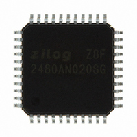
Z8F2480AN020SG
Manufacturer Part Number
Z8F2480AN020SG
Description
MCU 8BIT 24KB FLASH 44LQFP
Manufacturer
Zilog
Series
Encore!® XP®r
Specifications of Z8F2480AN020SG
Core Processor
Z8
Core Size
8-Bit
Speed
20MHz
Connectivity
I²C, IrDA, LIN, SPI, UART/USART
Peripherals
Brown-out Detect/Reset, LED, LVD, POR, PWM, Temp Sensor, WDT
Number Of I /o
37
Program Memory Size
24KB (24K x 8)
Program Memory Type
FLASH
Ram Size
3K x 8
Voltage - Supply (vcc/vdd)
1.8 V ~ 3.6 V
Data Converters
A/D 8x10b
Oscillator Type
Internal
Operating Temperature
0°C ~ 70°C
Package / Case
44-LQFP
Processor Series
Z8F248x
Core
eZ8
Data Bus Width
8 bit
Data Ram Size
2 KB
Interface Type
I2C, SPI, UART
Maximum Clock Frequency
20 MHz
Number Of Programmable I/os
37
Number Of Timers
3
Maximum Operating Temperature
+ 70 C
Mounting Style
SMD/SMT
Minimum Operating Temperature
0 C
On-chip Adc
10 bit, 8 Channel
For Use With
770-1002 - ISP 4PORT ZILOG Z8 ENCORE! MCU269-4643 - KIT DEV Z8 ENCORE XP 28-PIN269-4630 - DEV KIT FOR Z8 ENCORE 8K/4K269-4629 - KIT DEV Z8 ENCORE XP 28-PIN269-4628 - KIT DEV Z8 ENCORE XP 8-PIN
Lead Free Status / RoHS Status
Lead free / RoHS Compliant
Eeprom Size
-
Lead Free Status / Rohs Status
Details
Other names
269-4676
Available stocks
Company
Part Number
Manufacturer
Quantity
Price
Company:

Part Number:
Z8F2480AN020SG
Manufacturer:
Zilog
Quantity:
85


®
Z8 Encore! XP
F1680 Series
Product Specification
152
The Synch character is transmitted by writing a
to the Transmit Data Register (
55H
TDRE
must = 1 before writing). The Synch character is not transmitted by the hardware till the
Break is complete.
The Identifier character is transmitted by writing the appropriate value to the Transmit
Data Register (
must = 1 before writing).
TDRE
If the master is sending the response portion of the message, these data and checksum
characters are written to the Transmit Data Register when the
bit asserts. If the
TDRE
transmit data register is written after
asserts, but before
asserts, the hardware
TDRE
TXE
inserts one or two stop bits between each character as determined by the Stop bit in the
Control 0 Register. Additional idle time occurs between characters, if
asserts before
TXE
the next character is written.
If the selected slave is sending the response portion of the frame to the master, each
receive byte will be signalled by the receive data interrupt (
bit will be set in the
RDA
Status0 register). If the selected slave is sending the response to a different slave, the mas-
ter can ignore the response characters by deasserting the
bit in the Control 0 Register
REN
until the frame time slot is completed.
LIN SLEEP Mode
While the LIN bus is in the sleep state, the CPU can either be in low power STOP mode, in
HALT mode, or in normal operational state. Any device on the LIN bus may issue a Wake-
up message if it requires the master to initiate a LIN message frame. Following the Wake-
up message, the master wakes up and initiates a new message. A Wake-up message is
accomplished by pulling the bus Low for at least 250 µs but less than 5 ms. Transmitting a
character is one way to transmit the Wake-up message.
00H
If the CPU is in STOP mode, the LIN-UART is not active and the Wake-up message must
be detected by a GPIO edge detect Stop Mode Recovery. The duration of the Stop Mode
Recovery sequence may preclude making an accurate measurement of the Wake-up
message duration.
If the CPU is in HALT or OPERATIONAL mode, the LIN-UART (if enabled) times the
duration of the Wake-up and provides an interrupt following the end of the break sequence
if the duration is 3 bit times. The total duration of the Wake-up message in bit times may
be obtained by reading the
field in the Mode Select and Status register.
RxBreakLength
After a Wake-up message has been detected, the LIN-UART can be placed (by software)
either into LIN Master or LIN Slave Wait for Break states as appropriate. If the break
duration exceeds 15 bit times, the
field contains the value
. If the
RxBreakLength
Fh
LIN-UART is disabled, Wake-up message is detected via a port pin interrupt and timed by
software. If the device is in STOP mode, the High to Low transition on the port pin will
bring the device out of STOP mode.
The LIN Sleep state is selected by software setting
[1:0] = 00. The decision to
LinState
move from an active state to sleep state is based on the LIN messages as interpreted by
software.
PS025011-1010
P R E L I M I N A R Y
LIN-UART
Related parts for Z8F2480AN020SG
Image
Part Number
Description
Manufacturer
Datasheet
Request
R

Part Number:
Description:
Communication Controllers, ZILOG INTELLIGENT PERIPHERAL CONTROLLER (ZIP)
Manufacturer:
Zilog, Inc.
Datasheet:

Part Number:
Description:
KIT DEV FOR Z8 ENCORE 16K TO 64K
Manufacturer:
Zilog
Datasheet:

Part Number:
Description:
KIT DEV Z8 ENCORE XP 28-PIN
Manufacturer:
Zilog
Datasheet:

Part Number:
Description:
DEV KIT FOR Z8 ENCORE 8K/4K
Manufacturer:
Zilog
Datasheet:

Part Number:
Description:
KIT DEV Z8 ENCORE XP 28-PIN
Manufacturer:
Zilog
Datasheet:

Part Number:
Description:
DEV KIT FOR Z8 ENCORE 4K TO 8K
Manufacturer:
Zilog
Datasheet:
Part Number:
Description:
CMOS Z8 microcontroller. ROM 16 Kbytes, RAM 256 bytes, speed 16 MHz, 32 lines I/O, 3.0V to 5.5V
Manufacturer:
Zilog, Inc.
Datasheet:
Part Number:
Description:
Low-cost microcontroller. 512 bytes ROM, 61 bytes RAM, 8 MHz
Manufacturer:
Zilog, Inc.
Datasheet:
Part Number:
Description:
Z8 4K OTP Microcontroller
Manufacturer:
Zilog, Inc.
Datasheet:
Part Number:
Description:
CMOS SUPER8 ROMLESS MCU
Manufacturer:
Zilog, Inc.
Datasheet:
Part Number:
Description:
SL1866 CMOSZ8 OTP Microcontroller
Manufacturer:
Zilog, Inc.
Datasheet:
Part Number:
Description:
SL1866 CMOSZ8 OTP Microcontroller
Manufacturer:
Zilog, Inc.
Datasheet:
Part Number:
Description:
OTP (KB) = 1, RAM = 125, Speed = 12, I/O = 14, 8-bit Timers = 2, Comm Interfaces Other Features = Por, LV Protect, Voltage = 4.5-5.5V
Manufacturer:
Zilog, Inc.
Datasheet:
Part Number:
Description:
Manufacturer:
Zilog, Inc.
Datasheet: