Z8F2480AN020SG Zilog, Z8F2480AN020SG Datasheet - Page 311
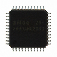
Z8F2480AN020SG
Manufacturer Part Number
Z8F2480AN020SG
Description
MCU 8BIT 24KB FLASH 44LQFP
Manufacturer
Zilog
Series
Encore!® XP®r
Specifications of Z8F2480AN020SG
Core Processor
Z8
Core Size
8-Bit
Speed
20MHz
Connectivity
I²C, IrDA, LIN, SPI, UART/USART
Peripherals
Brown-out Detect/Reset, LED, LVD, POR, PWM, Temp Sensor, WDT
Number Of I /o
37
Program Memory Size
24KB (24K x 8)
Program Memory Type
FLASH
Ram Size
3K x 8
Voltage - Supply (vcc/vdd)
1.8 V ~ 3.6 V
Data Converters
A/D 8x10b
Oscillator Type
Internal
Operating Temperature
0°C ~ 70°C
Package / Case
44-LQFP
Processor Series
Z8F248x
Core
eZ8
Data Bus Width
8 bit
Data Ram Size
2 KB
Interface Type
I2C, SPI, UART
Maximum Clock Frequency
20 MHz
Number Of Programmable I/os
37
Number Of Timers
3
Maximum Operating Temperature
+ 70 C
Mounting Style
SMD/SMT
Minimum Operating Temperature
0 C
On-chip Adc
10 bit, 8 Channel
For Use With
770-1002 - ISP 4PORT ZILOG Z8 ENCORE! MCU269-4643 - KIT DEV Z8 ENCORE XP 28-PIN269-4630 - DEV KIT FOR Z8 ENCORE 8K/4K269-4629 - KIT DEV Z8 ENCORE XP 28-PIN269-4628 - KIT DEV Z8 ENCORE XP 8-PIN
Lead Free Status / RoHS Status
Lead free / RoHS Compliant
Eeprom Size
-
Lead Free Status / Rohs Status
Details
Other names
269-4676
Available stocks
Company
Part Number
Manufacturer
Quantity
Price
Company:

Part Number:
Z8F2480AN020SG
Manufacturer:
Zilog
Quantity:
85


PS025011-1010
•
•
•
•
can be written 1–65536 bytes at a time (65536 bytes can be written by setting size to 0).
The on-chip Flash Controller must be written and unlocked for the programming operation
to occur. If the Flash Controller is not unlocked, the data is discarded. If the device is not
in DEBUG mode or if the Read Protect Option Bit is enabled, the data is discarded.
DBG
DBG
DBG
DBG
DBG
DBG
Read Program Memory (0BH)—The Read Program Memory command reads data
from Program Memory. This command is equivalent to the LDC and LDCI instructions.
Data can be read 1–65536 bytes at a time (65536 bytes can be read by setting size to 0). If
the device is not in DEBUG mode or if the Read Protect Option Bit is enabled, this com-
mand returns
DBG
DBG
DBG
DBG
DBG
DBG
Write Data Memory (0CH)—The Write Data Memory command writes data to Data
Memory. This command is equivalent to the LDE and LDEI instructions. Data is written
1–65536 bytes at a time (65536 bytes can be written by setting size to 0). If the device is
not in DEBUG mode or if the Read Protect Option Bit is enabled, the data is discarded.
DBG
DBG
DBG
DBG
DBG
DBG
Read Data Memory (0DH)—The Read Data Memory command reads from Data
Memory. This command is equivalent to the LDE and LDEI instructions. Data can be read
1 to 65536 bytes at a time (65536 bytes can be read by setting size to 0). If the device is
not in DEBUG mode, this command returns
DBG
DBG
DBG
DBG
DBG
DBG
Read Program Memory CRC (0EH)—The Read Program Memory CRC command
computes and returns the CRC (cyclic redundancy check) of Program Memory using
0AH
Program Memory Address[15:8]
Program Memory Address[7:0]
Size[15:8]
Size[7:0]
1-65536 data bytes
0BH
Program Memory Address[15:8]
Program Memory Address[7:0]
Size[15:8]
Size[7:0]
1-65536 data bytes
0CH
Data Memory Address[15:8]
Data Memory Address[7:0]
Size[15:8]
Size[7:0]
1-65536 data bytes
0DH
Data Memory Address[15:8]
Data Memory Address[7:0]
Size[15:8]
Size[7:0]
1-65536 data bytes
FFH
for the data.
P R E L I M I N A R Y
FFH
for the data.
Z8 Encore! XP
Product Specification
®
On-Chip Debugger
F1680 Series
297
Related parts for Z8F2480AN020SG
Image
Part Number
Description
Manufacturer
Datasheet
Request
R

Part Number:
Description:
Communication Controllers, ZILOG INTELLIGENT PERIPHERAL CONTROLLER (ZIP)
Manufacturer:
Zilog, Inc.
Datasheet:

Part Number:
Description:
KIT DEV FOR Z8 ENCORE 16K TO 64K
Manufacturer:
Zilog
Datasheet:

Part Number:
Description:
KIT DEV Z8 ENCORE XP 28-PIN
Manufacturer:
Zilog
Datasheet:

Part Number:
Description:
DEV KIT FOR Z8 ENCORE 8K/4K
Manufacturer:
Zilog
Datasheet:

Part Number:
Description:
KIT DEV Z8 ENCORE XP 28-PIN
Manufacturer:
Zilog
Datasheet:

Part Number:
Description:
DEV KIT FOR Z8 ENCORE 4K TO 8K
Manufacturer:
Zilog
Datasheet:
Part Number:
Description:
CMOS Z8 microcontroller. ROM 16 Kbytes, RAM 256 bytes, speed 16 MHz, 32 lines I/O, 3.0V to 5.5V
Manufacturer:
Zilog, Inc.
Datasheet:
Part Number:
Description:
Low-cost microcontroller. 512 bytes ROM, 61 bytes RAM, 8 MHz
Manufacturer:
Zilog, Inc.
Datasheet:
Part Number:
Description:
Z8 4K OTP Microcontroller
Manufacturer:
Zilog, Inc.
Datasheet:
Part Number:
Description:
CMOS SUPER8 ROMLESS MCU
Manufacturer:
Zilog, Inc.
Datasheet:
Part Number:
Description:
SL1866 CMOSZ8 OTP Microcontroller
Manufacturer:
Zilog, Inc.
Datasheet:
Part Number:
Description:
SL1866 CMOSZ8 OTP Microcontroller
Manufacturer:
Zilog, Inc.
Datasheet:
Part Number:
Description:
OTP (KB) = 1, RAM = 125, Speed = 12, I/O = 14, 8-bit Timers = 2, Comm Interfaces Other Features = Por, LV Protect, Voltage = 4.5-5.5V
Manufacturer:
Zilog, Inc.
Datasheet:
Part Number:
Description:
Manufacturer:
Zilog, Inc.
Datasheet: