Z8F2480AN020SG Zilog, Z8F2480AN020SG Datasheet - Page 298
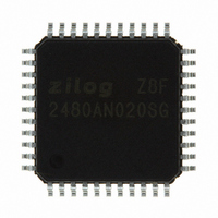
Z8F2480AN020SG
Manufacturer Part Number
Z8F2480AN020SG
Description
MCU 8BIT 24KB FLASH 44LQFP
Manufacturer
Zilog
Series
Encore!® XP®r
Specifications of Z8F2480AN020SG
Core Processor
Z8
Core Size
8-Bit
Speed
20MHz
Connectivity
I²C, IrDA, LIN, SPI, UART/USART
Peripherals
Brown-out Detect/Reset, LED, LVD, POR, PWM, Temp Sensor, WDT
Number Of I /o
37
Program Memory Size
24KB (24K x 8)
Program Memory Type
FLASH
Ram Size
3K x 8
Voltage - Supply (vcc/vdd)
1.8 V ~ 3.6 V
Data Converters
A/D 8x10b
Oscillator Type
Internal
Operating Temperature
0°C ~ 70°C
Package / Case
44-LQFP
Processor Series
Z8F248x
Core
eZ8
Data Bus Width
8 bit
Data Ram Size
2 KB
Interface Type
I2C, SPI, UART
Maximum Clock Frequency
20 MHz
Number Of Programmable I/os
37
Number Of Timers
3
Maximum Operating Temperature
+ 70 C
Mounting Style
SMD/SMT
Minimum Operating Temperature
0 C
On-chip Adc
10 bit, 8 Channel
For Use With
770-1002 - ISP 4PORT ZILOG Z8 ENCORE! MCU269-4643 - KIT DEV Z8 ENCORE XP 28-PIN269-4630 - DEV KIT FOR Z8 ENCORE 8K/4K269-4629 - KIT DEV Z8 ENCORE XP 28-PIN269-4628 - KIT DEV Z8 ENCORE XP 8-PIN
Lead Free Status / RoHS Status
Lead free / RoHS Compliant
Eeprom Size
-
Lead Free Status / Rohs Status
Details
Other names
269-4676
Available stocks
Company
Part Number
Manufacturer
Quantity
Price
Company:

Part Number:
Z8F2480AN020SG
Manufacturer:
Zilog
Quantity:
85


PS025011-1010
Power Failure Protection
Optimizing NVDS Memory Usage for Execution Speed
The NVDS routines employ error checking mechanisms to ensure a power failure endan-
gers only the most recently written byte. Bytes previously written to the array are not per-
turbed. For this protection to function, the VBO must be enabled (see
on page 45) and configured for a threshold voltage of 2.4 V or greater (see
Address Space
A System Reset (such as a pin reset or watchdog timer reset) that occurs during a write
operation also perturbs the byte currently being written. All other bytes in the array are
unperturbed.
As listed in
trade-off for minimizing the frequency of writes that require post-write page erases. The
NVDS read time of address N is a function of the number of writes to addresses other than
N since the most recent write to address N, as well as the number of writes since the most
recent page erase. Neglecting effects caused by page erases and results caused by the
initial condition in which the NVDS is blank, a rule of thumb is that every write since the
most recent page erase causes read times of unwritten addresses to increase by 0.8 s, up
to a maximum of 258 s.
If NVDS read performance is critical to your software architecture, you can optimize your
code for speed by using either of the methods listed below.
1. Periodically refresh all addresses that are used. This is the most useful method. The
2. Use as few unique addresses as possible. This helps to optimize the impact of
optimal use of NVDS in terms of speed is to rotate the writes evenly among all
addresses planned to use, bringing all reads closer to the minimum read time. Because
the minimum read time is much less than the write time, however, actual speed
benefits are not always realized.
refreshing.
Table 161.NVDS Read Time
Operation
Read
Write
Illegal Read
Illegal Write
Table
on page 272).
161, the NVDS read time varies drastically, this discrepancy being a
P R E L I M I N A R Y
Minimum
Latency (
71
126
6
7
s
)
Maximum
Latency (
258
6
7
136
Z8 Encore! XP
s
)
Product Specification
Non-Volatile Data Storage
Low-Power Modes
®
F1680 Series
Trim Bit
284
Related parts for Z8F2480AN020SG
Image
Part Number
Description
Manufacturer
Datasheet
Request
R

Part Number:
Description:
Communication Controllers, ZILOG INTELLIGENT PERIPHERAL CONTROLLER (ZIP)
Manufacturer:
Zilog, Inc.
Datasheet:

Part Number:
Description:
KIT DEV FOR Z8 ENCORE 16K TO 64K
Manufacturer:
Zilog
Datasheet:

Part Number:
Description:
KIT DEV Z8 ENCORE XP 28-PIN
Manufacturer:
Zilog
Datasheet:

Part Number:
Description:
DEV KIT FOR Z8 ENCORE 8K/4K
Manufacturer:
Zilog
Datasheet:

Part Number:
Description:
KIT DEV Z8 ENCORE XP 28-PIN
Manufacturer:
Zilog
Datasheet:

Part Number:
Description:
DEV KIT FOR Z8 ENCORE 4K TO 8K
Manufacturer:
Zilog
Datasheet:
Part Number:
Description:
CMOS Z8 microcontroller. ROM 16 Kbytes, RAM 256 bytes, speed 16 MHz, 32 lines I/O, 3.0V to 5.5V
Manufacturer:
Zilog, Inc.
Datasheet:
Part Number:
Description:
Low-cost microcontroller. 512 bytes ROM, 61 bytes RAM, 8 MHz
Manufacturer:
Zilog, Inc.
Datasheet:
Part Number:
Description:
Z8 4K OTP Microcontroller
Manufacturer:
Zilog, Inc.
Datasheet:
Part Number:
Description:
CMOS SUPER8 ROMLESS MCU
Manufacturer:
Zilog, Inc.
Datasheet:
Part Number:
Description:
SL1866 CMOSZ8 OTP Microcontroller
Manufacturer:
Zilog, Inc.
Datasheet:
Part Number:
Description:
SL1866 CMOSZ8 OTP Microcontroller
Manufacturer:
Zilog, Inc.
Datasheet:
Part Number:
Description:
OTP (KB) = 1, RAM = 125, Speed = 12, I/O = 14, 8-bit Timers = 2, Comm Interfaces Other Features = Por, LV Protect, Voltage = 4.5-5.5V
Manufacturer:
Zilog, Inc.
Datasheet:
Part Number:
Description:
Manufacturer:
Zilog, Inc.
Datasheet: