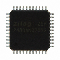
Z8F2480AN020SG Zilog, Z8F2480AN020SG Datasheet - Page 307

Z8F2480AN020SG
Manufacturer Part Number
Z8F2480AN020SG
Description
MCU 8BIT 24KB FLASH 44LQFP
Manufacturer
Zilog
Series
Encore!® XP®r
Specifications of Z8F2480AN020SG
Core Processor
Z8
Core Size
8-Bit
Speed
20MHz
Connectivity
I²C, IrDA, LIN, SPI, UART/USART
Peripherals
Brown-out Detect/Reset, LED, LVD, POR, PWM, Temp Sensor, WDT
Number Of I /o
37
Program Memory Size
24KB (24K x 8)
Program Memory Type
FLASH
Ram Size
3K x 8
Voltage - Supply (vcc/vdd)
1.8 V ~ 3.6 V
Data Converters
A/D 8x10b
Oscillator Type
Internal
Operating Temperature
0°C ~ 70°C
Package / Case
44-LQFP
Processor Series
Z8F248x
Core
eZ8
Data Bus Width
8 bit
Data Ram Size
2 KB
Interface Type
I2C, SPI, UART
Maximum Clock Frequency
20 MHz
Number Of Programmable I/os
37
Number Of Timers
3
Maximum Operating Temperature
+ 70 C
Mounting Style
SMD/SMT
Minimum Operating Temperature
0 C
On-chip Adc
10 bit, 8 Channel
For Use With
770-1002 - ISP 4PORT ZILOG Z8 ENCORE! MCU269-4643 - KIT DEV Z8 ENCORE XP 28-PIN269-4630 - DEV KIT FOR Z8 ENCORE 8K/4K269-4629 - KIT DEV Z8 ENCORE XP 28-PIN269-4628 - KIT DEV Z8 ENCORE XP 8-PIN
Lead Free Status / RoHS Status
Lead free / RoHS Compliant
Eeprom Size
-
Lead Free Status / Rohs Status
Details
Other names
269-4676
Available stocks
Company
Part Number
Manufacturer
Quantity
Price
Company:
Part Number:
Z8F2480AN020SG
Manufacturer:
Zilog
Quantity:
85
- Current page: 307 of 399
- Download datasheet (19Mb)
On-Chip Debugger Commands
PS025011-1010
Caution:
be generated when the program counter matches the value in the OCDCNTR register
before executing the instruction at the location of the program counter.
Because this register is overwritten by various OCD commands, it must only be used to
generate temporary breakpoints, such as stepping over CALL instructions or running to a
specific instruction and stopping.
When the OCDCNTR register is read, it returns the inverse of the data in this register. The
OCDCNTR register is only decremented when counting. The mode where it counts the
number of clock cycles in between execution is achieved by counting down from its max-
imum count. When the OCDCNTR register is read, the counter appears to have counted
up because its value is inverted. The value in this register is always inverted when it is
read. If this register is used as a hardware breakpoint, the value read from this register will
be the inverse of the data actually in the register.
The host communicates to the On-Chip Debugger by sending OCD commands using the
DBG interface. During normal operation, only a subset of the OCD commands are
available. In Debug mode, all OCD commands become available unless the user
code is protected by programming the Flash Read Protect Option Bit (FRP). The Flash
Read Protect Option Bit prevents the code in memory from being read out of the Z8
Encore! XP F1680 Series device. When this option is enabled, several of the OCD
commands are disabled. When the Read Protect Option Bit is enabled and the Information
Area Write Protect bits are enabled, asserting the TESTMODE pad does NOT put the
Table 163
command is described in further detail in the bulleted list following the table.
The table indicates those commands that operate when the device is not in DEBUG mode
Z8 Encore! XP F1680 Series in Flash Test mode.
The OCDCNTR register is used by many of the OCD commands. It counts the
number of bytes for the register and memory read/write commands. It retains
the residual value when generating the CRC. If the OCDCNTR is used to gen-
erate a BRK, its value must be written as a final step before leaving DEBUG
mode.
contains a summary of the On-Chip Debugger commands. Each OCD
P R E L I M I N A R Y
Z8 Encore! XP
Product Specification
®
On-Chip Debugger
F1680 Series
293
Related parts for Z8F2480AN020SG
Image
Part Number
Description
Manufacturer
Datasheet
Request
R

Part Number:
Description:
Communication Controllers, ZILOG INTELLIGENT PERIPHERAL CONTROLLER (ZIP)
Manufacturer:
Zilog, Inc.
Datasheet:

Part Number:
Description:
KIT DEV FOR Z8 ENCORE 16K TO 64K
Manufacturer:
Zilog
Datasheet:

Part Number:
Description:
KIT DEV Z8 ENCORE XP 28-PIN
Manufacturer:
Zilog
Datasheet:

Part Number:
Description:
DEV KIT FOR Z8 ENCORE 8K/4K
Manufacturer:
Zilog
Datasheet:

Part Number:
Description:
KIT DEV Z8 ENCORE XP 28-PIN
Manufacturer:
Zilog
Datasheet:

Part Number:
Description:
DEV KIT FOR Z8 ENCORE 4K TO 8K
Manufacturer:
Zilog
Datasheet:

Part Number:
Description:
CMOS Z8 microcontroller. ROM 16 Kbytes, RAM 256 bytes, speed 16 MHz, 32 lines I/O, 3.0V to 5.5V
Manufacturer:
Zilog, Inc.
Datasheet:

Part Number:
Description:
Low-cost microcontroller. 512 bytes ROM, 61 bytes RAM, 8 MHz
Manufacturer:
Zilog, Inc.
Datasheet:

Part Number:
Description:
Z8 4K OTP Microcontroller
Manufacturer:
Zilog, Inc.
Datasheet:

Part Number:
Description:
CMOS SUPER8 ROMLESS MCU
Manufacturer:
Zilog, Inc.
Datasheet:

Part Number:
Description:
SL1866 CMOSZ8 OTP Microcontroller
Manufacturer:
Zilog, Inc.
Datasheet:

Part Number:
Description:
SL1866 CMOSZ8 OTP Microcontroller
Manufacturer:
Zilog, Inc.
Datasheet:

Part Number:
Description:
OTP (KB) = 1, RAM = 125, Speed = 12, I/O = 14, 8-bit Timers = 2, Comm Interfaces Other Features = Por, LV Protect, Voltage = 4.5-5.5V
Manufacturer:
Zilog, Inc.
Datasheet:

Part Number:
Description:
Manufacturer:
Zilog, Inc.
Datasheet:


