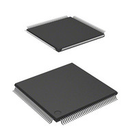
DF2161BVTE10 Renesas Electronics America, DF2161BVTE10 Datasheet - Page 398

DF2161BVTE10
Manufacturer Part Number
DF2161BVTE10
Description
MCU 3V 128K 144-TQFP
Manufacturer
Renesas Electronics America
Series
H8® H8S/2100r
Datasheet
1.DF2160BVT10V.pdf
(847 pages)
Specifications of DF2161BVTE10
Core Processor
H8S/2000
Core Size
16-Bit
Speed
10MHz
Connectivity
Host Interface (LPC), I²C, IrDA, SCI, X-Bus
Peripherals
PWM, WDT
Number Of I /o
114
Program Memory Size
128KB (128K x 8)
Program Memory Type
FLASH
Ram Size
4K x 8
Voltage - Supply (vcc/vdd)
2.7 V ~ 3.6 V
Data Converters
A/D 8x10b; D/A 2x8b
Oscillator Type
Internal
Operating Temperature
-20°C ~ 75°C
Package / Case
144-TQFP, 144-VQFP
Lead Free Status / RoHS Status
Contains lead / RoHS non-compliant
Eeprom Size
-
Other names
HD64F2161BVTE10
HD64F2161BVTE10
HD64F2161BVTE10
- Current page: 398 of 847
- Download datasheet (5Mb)
Section 13 Timer Connection
13.4.8
With the VSYNCO output, the meaning of the signal source to be selected and use or non-use of
modification varies according to the IVI signal source and the waveform required by external
circuitry. The VSYNCO output modes are shown in table 13.11.
Table 13.11 VSYNCO Output Modes
Mode
No signal
S-on-G
mode or
composite
mode
Rev. 3.00 Mar 21, 2006 page 342 of 788
REJ09B0300-0300
VSYNCO Output
IVI Signal
VFBACKI
input
PDC signal
IVO Signal
IVI signal (without fall
modification or IHI
synchronization)
IVI signal (without fall
modification, with IHI
synchronization)
IVI signal (with fall
modification, without IHI
synchronization)
IVI signal (with fall
modification and IHI
synchronization)
IVG signal
IVI signal (without fall
modification or IHI
synchronization)
IVI signal (without fall
modification, with IHI
synchronization)
IVI signal (with fall
modification, without IHI
synchronization)
IVI signal (with fall
modification and IHI
synchronization)
IVG signal
Meaning of IVO Signal
VFBACKI input is output directly
Meaningless unless VFBACKI input is
synchronized with HFBACKI input
VFBACKI input fall is modified before output
VFBACKI input fall is modified and signal is
synchronized with HFBACKI input before
output
Internal synchronization signal is output
CSYNCI/HSYNCI input (composite
synchronization signal) vertical
synchronization signal part is separated
before output
CSYNCI/HSYNCI input (composite
synchronization signal) vertical
synchronization signal part is separated, and
signal is synchronized with CSYNCI/HSYNCI
input before output
CSYNCI/HSYNCI input (composite
synchronization signal) vertical
synchronization signal part is separated, and
fall is modified before output
CSYNCI/HSYNCI input (composite
synchronization signal) vertical
synchronization signal part is separated, fall is
modified, and signal is synchronized with
CSYNCI/HSYNCI input before output
Internal synchronization signal is output
Related parts for DF2161BVTE10
Image
Part Number
Description
Manufacturer
Datasheet
Request
R

Part Number:
Description:
KIT STARTER FOR M16C/29
Manufacturer:
Renesas Electronics America
Datasheet:

Part Number:
Description:
KIT STARTER FOR R8C/2D
Manufacturer:
Renesas Electronics America
Datasheet:

Part Number:
Description:
R0K33062P STARTER KIT
Manufacturer:
Renesas Electronics America
Datasheet:

Part Number:
Description:
KIT STARTER FOR R8C/23 E8A
Manufacturer:
Renesas Electronics America
Datasheet:

Part Number:
Description:
KIT STARTER FOR R8C/25
Manufacturer:
Renesas Electronics America
Datasheet:

Part Number:
Description:
KIT STARTER H8S2456 SHARPE DSPLY
Manufacturer:
Renesas Electronics America
Datasheet:

Part Number:
Description:
KIT STARTER FOR R8C38C
Manufacturer:
Renesas Electronics America
Datasheet:

Part Number:
Description:
KIT STARTER FOR R8C35C
Manufacturer:
Renesas Electronics America
Datasheet:

Part Number:
Description:
KIT STARTER FOR R8CL3AC+LCD APPS
Manufacturer:
Renesas Electronics America
Datasheet:

Part Number:
Description:
KIT STARTER FOR RX610
Manufacturer:
Renesas Electronics America
Datasheet:

Part Number:
Description:
KIT STARTER FOR R32C/118
Manufacturer:
Renesas Electronics America
Datasheet:

Part Number:
Description:
KIT DEV RSK-R8C/26-29
Manufacturer:
Renesas Electronics America
Datasheet:

Part Number:
Description:
KIT STARTER FOR SH7124
Manufacturer:
Renesas Electronics America
Datasheet:

Part Number:
Description:
KIT STARTER FOR H8SX/1622
Manufacturer:
Renesas Electronics America
Datasheet:

Part Number:
Description:
KIT DEV FOR SH7203
Manufacturer:
Renesas Electronics America
Datasheet:


