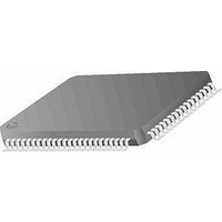
MC9S12E64CFU Freescale Semiconductor, MC9S12E64CFU Datasheet - Page 168

MC9S12E64CFU
Manufacturer Part Number
MC9S12E64CFU
Description
IC MCU 64K FLASH 25MHZ 80-QFP
Manufacturer
Freescale Semiconductor
Series
HCS12r
Specifications of MC9S12E64CFU
Core Processor
HCS12
Core Size
16-Bit
Speed
25MHz
Connectivity
EBI/EMI, I²C, SCI, SPI
Peripherals
POR, PWM, WDT
Number Of I /o
60
Program Memory Size
64KB (64K x 8)
Program Memory Type
FLASH
Ram Size
4K x 8
Voltage - Supply (vcc/vdd)
2.35 V ~ 2.75 V
Data Converters
A/D 16x10b; D/A 2x8b
Oscillator Type
Internal
Operating Temperature
-40°C ~ 85°C
Package / Case
80-QFP
Data Bus Width
16 bit
Data Ram Size
4 KB
Interface Type
SCI, SPI
Maximum Clock Frequency
25 MHz
Number Of Programmable I/os
60
Number Of Timers
16 bit
Maximum Operating Temperature
+ 85 C
Mounting Style
SMD/SMT
Minimum Operating Temperature
- 40 C
On-chip Adc
10 bit
On-chip Dac
8 bit, 2 Channel
For Use With
M68EVB912E128 - BOARD EVAL FOR MC9S12E128/64
Lead Free Status / RoHS Status
Contains lead / RoHS non-compliant
Eeprom Size
-
Lead Free Status / Rohs Status
No RoHS Version Available
Available stocks
Company
Part Number
Manufacturer
Quantity
Price
Company:
Part Number:
MC9S12E64CFU
Manufacturer:
Freescale Semiconductor
Quantity:
10 000
Company:
Part Number:
MC9S12E64CFUE
Manufacturer:
Freescale Semiconductor
Quantity:
10 000
Part Number:
MC9S12E64CFUE
Manufacturer:
FREESCALE
Quantity:
20 000
Company:
Part Number:
MC9S12E64CFUER
Manufacturer:
Freescale Semiconductor
Quantity:
10 000
- Current page: 168 of 606
- Download datasheet (4Mb)
Chapter 4 Clocks and Reset Generator (CRGV4)
4.2.3
RESET is an active low bidirectional reset pin. As an input it initializes the MCU asynchronously to a
known start-up state. As an open-drain output it indicates that an system reset (internal to MCU) has been
triggered.
4.3
This section provides a detailed description of all registers accessible in the CRGV4.
4.3.1
Table 4-1
168
1
2
3
CTFLG is intended for factory test purposes only.
FORBYP is intended for factory test purposes only.
CTCTL is intended for factory test purposes only.
Memory Map and Register Definition
Address
gives an overview on all CRGV4 registers.
0x000A
0x000B
0x0000
0x0001
0x0002
0x0003
0x0004
0x0005
0x0006
0x0007
0x0008
0x0009
Offset
RESET — Reset Pin
Module Memory Map
CRG Synthesizer Register (SYNR)
CRG Reference Divider Register (REFDV)
CRG Test Flags Register (CTFLG)
CRG Flags Register (CRGFLG)
CRG Interrupt Enable Register (CRGINT)
CRG Clock Select Register (CLKSEL)
CRG PLL Control Register (PLLCTL)
CRG RTI Control Register (RTICTL)
CRG COP Control Register (COPCTL)
CRG Force and Bypass Test Register (FORBYP)
CRG Test Control Register (CTCTL)
CRG COP Arm/Timer Reset (ARMCOP)
Figure 4-2. PLL Loop Filter Connections
MCU
MC9S12E128 Data Sheet, Rev. 1.07
Table 4-1. CRGV4 Memory Map
XFC
1
3
Use
RS
CS
2
CP
V
DDPLL
Freescale Semiconductor
Access
R/W
R/W
R/W
R/W
R/W
R/W
R/W
R/W
R/W
R/W
R/W
R/W
Related parts for MC9S12E64CFU
Image
Part Number
Description
Manufacturer
Datasheet
Request
R
Part Number:
Description:
Manufacturer:
Freescale Semiconductor, Inc
Datasheet:
Part Number:
Description:
Manufacturer:
Freescale Semiconductor, Inc
Datasheet:
Part Number:
Description:
Manufacturer:
Freescale Semiconductor, Inc
Datasheet:
Part Number:
Description:
Manufacturer:
Freescale Semiconductor, Inc
Datasheet:
Part Number:
Description:
Manufacturer:
Freescale Semiconductor, Inc
Datasheet:
Part Number:
Description:
Manufacturer:
Freescale Semiconductor, Inc
Datasheet:
Part Number:
Description:
Manufacturer:
Freescale Semiconductor, Inc
Datasheet:
Part Number:
Description:
Manufacturer:
Freescale Semiconductor, Inc
Datasheet:
Part Number:
Description:
Manufacturer:
Freescale Semiconductor, Inc
Datasheet:
Part Number:
Description:
Manufacturer:
Freescale Semiconductor, Inc
Datasheet:
Part Number:
Description:
Manufacturer:
Freescale Semiconductor, Inc
Datasheet:
Part Number:
Description:
Manufacturer:
Freescale Semiconductor, Inc
Datasheet:
Part Number:
Description:
Manufacturer:
Freescale Semiconductor, Inc
Datasheet:
Part Number:
Description:
Manufacturer:
Freescale Semiconductor, Inc
Datasheet:
Part Number:
Description:
Manufacturer:
Freescale Semiconductor, Inc
Datasheet:


