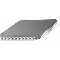
MC9S12E64CFU Freescale Semiconductor, MC9S12E64CFU Datasheet - Page 180

MC9S12E64CFU
Manufacturer Part Number
MC9S12E64CFU
Description
IC MCU 64K FLASH 25MHZ 80-QFP
Manufacturer
Freescale Semiconductor
Series
HCS12r
Specifications of MC9S12E64CFU
Core Processor
HCS12
Core Size
16-Bit
Speed
25MHz
Connectivity
EBI/EMI, I²C, SCI, SPI
Peripherals
POR, PWM, WDT
Number Of I /o
60
Program Memory Size
64KB (64K x 8)
Program Memory Type
FLASH
Ram Size
4K x 8
Voltage - Supply (vcc/vdd)
2.35 V ~ 2.75 V
Data Converters
A/D 16x10b; D/A 2x8b
Oscillator Type
Internal
Operating Temperature
-40°C ~ 85°C
Package / Case
80-QFP
Data Bus Width
16 bit
Data Ram Size
4 KB
Interface Type
SCI, SPI
Maximum Clock Frequency
25 MHz
Number Of Programmable I/os
60
Number Of Timers
16 bit
Maximum Operating Temperature
+ 85 C
Mounting Style
SMD/SMT
Minimum Operating Temperature
- 40 C
On-chip Adc
10 bit
On-chip Dac
8 bit, 2 Channel
For Use With
M68EVB912E128 - BOARD EVAL FOR MC9S12E128/64
Lead Free Status / RoHS Status
Contains lead / RoHS non-compliant
Eeprom Size
-
Lead Free Status / Rohs Status
No RoHS Version Available
Available stocks
Company
Part Number
Manufacturer
Quantity
Price
Company:
Part Number:
MC9S12E64CFU
Manufacturer:
Freescale Semiconductor
Quantity:
10 000
Company:
Part Number:
MC9S12E64CFUE
Manufacturer:
Freescale Semiconductor
Quantity:
10 000
Part Number:
MC9S12E64CFUE
Manufacturer:
FREESCALE
Quantity:
20 000
Company:
Part Number:
MC9S12E64CFUER
Manufacturer:
Freescale Semiconductor
Quantity:
10 000
- Current page: 180 of 606
- Download datasheet (4Mb)
Chapter 4 Clocks and Reset Generator (CRGV4)
4.3.2.12
This register is used to restart the COP time-out period.
Read: always reads 0x0000
Write: anytime
When the COP is disabled (CR[2:0] = “000”) writing to this register has no effect.
When the COP is enabled by setting CR[2:0] nonzero, the following applies:
4.4
This section gives detailed informations on the internal operation of the design.
4.4.1
The PLL is used to run the MCU from a different time base than the incoming OSCCLK. For increased
flexibility, OSCCLK can be divided in a range of 1 to 16 to generate the reference frequency. This offers
a finer multiplication granularity. The PLL can multiply this reference clock by a multiple of 2, 4, 6,...
126,128 based on the SYNR register.
The PLL is a frequency generator that operates in either acquisition mode or tracking mode, depending on
the difference between the output frequency and the target frequency. The PLL can change between
acquisition and tracking modes either automatically or manually.
180
Reset
W
R
Writing any value other than 0x0055 or 0x00AA causes a COP reset. To restart the COP time-out
period you must write 0x0055 followed by a write of 0x00AA. Other instructions may be executed
between these writes but the sequence (0x0055, 0x00AA) must be completed prior to COP end of
time-out period to avoid a COP reset. Sequences of 0x0055 writes or sequences of 0x00AA writes
are allowed. When the WCOP bit is set, 0x0055 and 0x00AA writes must be done in the last 25%
of the selected time-out period; writing any value in the first 75% of the selected period will cause
a COP reset.
Functional Description
Phase Locked Loop (PLL)
Bit 7
CRG COP Timer Arm/Reset Register (ARMCOP)
0
0
7
Although it is possible to set the two dividers to command a very high clock
frequency, do not exceed the specified bus frequency limit for the MCU.
If (PLLSEL = 1), Bus Clock = PLLCLK / 2
Bit 6
0
0
6
PLLCLK
Figure 4-15. ARMCOP Register Diagram
Bit 5
MC9S12E128 Data Sheet, Rev. 1.07
0
0
5
=
2 OSCCLK
CAUTION
Bit 4
0
0
4
---------------------------------- -
REFDV
SYNR
Bit 3
0
0
3
+
+
1
1
Bit 2
0
0
2
Freescale Semiconductor
Bit 1
0
0
1
Bit 0
0
0
0
Related parts for MC9S12E64CFU
Image
Part Number
Description
Manufacturer
Datasheet
Request
R
Part Number:
Description:
Manufacturer:
Freescale Semiconductor, Inc
Datasheet:
Part Number:
Description:
Manufacturer:
Freescale Semiconductor, Inc
Datasheet:
Part Number:
Description:
Manufacturer:
Freescale Semiconductor, Inc
Datasheet:
Part Number:
Description:
Manufacturer:
Freescale Semiconductor, Inc
Datasheet:
Part Number:
Description:
Manufacturer:
Freescale Semiconductor, Inc
Datasheet:
Part Number:
Description:
Manufacturer:
Freescale Semiconductor, Inc
Datasheet:
Part Number:
Description:
Manufacturer:
Freescale Semiconductor, Inc
Datasheet:
Part Number:
Description:
Manufacturer:
Freescale Semiconductor, Inc
Datasheet:
Part Number:
Description:
Manufacturer:
Freescale Semiconductor, Inc
Datasheet:
Part Number:
Description:
Manufacturer:
Freescale Semiconductor, Inc
Datasheet:
Part Number:
Description:
Manufacturer:
Freescale Semiconductor, Inc
Datasheet:
Part Number:
Description:
Manufacturer:
Freescale Semiconductor, Inc
Datasheet:
Part Number:
Description:
Manufacturer:
Freescale Semiconductor, Inc
Datasheet:
Part Number:
Description:
Manufacturer:
Freescale Semiconductor, Inc
Datasheet:
Part Number:
Description:
Manufacturer:
Freescale Semiconductor, Inc
Datasheet:


