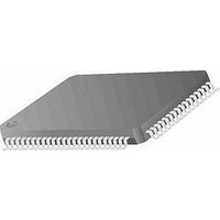
MC9S12E64CFU Freescale Semiconductor, MC9S12E64CFU Datasheet - Page 287

MC9S12E64CFU
Manufacturer Part Number
MC9S12E64CFU
Description
IC MCU 64K FLASH 25MHZ 80-QFP
Manufacturer
Freescale Semiconductor
Series
HCS12r
Specifications of MC9S12E64CFU
Core Processor
HCS12
Core Size
16-Bit
Speed
25MHz
Connectivity
EBI/EMI, I²C, SCI, SPI
Peripherals
POR, PWM, WDT
Number Of I /o
60
Program Memory Size
64KB (64K x 8)
Program Memory Type
FLASH
Ram Size
4K x 8
Voltage - Supply (vcc/vdd)
2.35 V ~ 2.75 V
Data Converters
A/D 16x10b; D/A 2x8b
Oscillator Type
Internal
Operating Temperature
-40°C ~ 85°C
Package / Case
80-QFP
Data Bus Width
16 bit
Data Ram Size
4 KB
Interface Type
SCI, SPI
Maximum Clock Frequency
25 MHz
Number Of Programmable I/os
60
Number Of Timers
16 bit
Maximum Operating Temperature
+ 85 C
Mounting Style
SMD/SMT
Minimum Operating Temperature
- 40 C
On-chip Adc
10 bit
On-chip Dac
8 bit, 2 Channel
For Use With
M68EVB912E128 - BOARD EVAL FOR MC9S12E128/64
Lead Free Status / RoHS Status
Contains lead / RoHS non-compliant
Eeprom Size
-
Lead Free Status / Rohs Status
No RoHS Version Available
Available stocks
Company
Part Number
Manufacturer
Quantity
Price
Company:
Part Number:
MC9S12E64CFU
Manufacturer:
Freescale Semiconductor
Quantity:
10 000
Company:
Part Number:
MC9S12E64CFUE
Manufacturer:
Freescale Semiconductor
Quantity:
10 000
Part Number:
MC9S12E64CFUE
Manufacturer:
FREESCALE
Quantity:
20 000
Company:
Part Number:
MC9S12E64CFUER
Manufacturer:
Freescale Semiconductor
Quantity:
10 000
- Current page: 287 of 606
- Download datasheet (4Mb)
The SPI Data Register is both the input and output register for SPI data. A write to this register allows a
data byte to be queued and transmitted. For a SPI configured as a master, a queued data byte is transmitted
immediately after the previous transmission has completed. The SPI Transmitter Empty Flag SPTEF in
the SPISR register indicates when the SPI Data Register is ready to accept new data.
Reading the data can occur anytime from after the SPIF is set to before the end of the next transfer. If the
SPIF is not serviced by the end of the successive transfers, those data bytes are lost and the data within the
SPIDR retains the first byte until SPIF is serviced.
9.4
The SPI module allows a duplex, synchronous, serial communication between the MCU and peripheral
devices. Software can poll the SPI status flags or SPI operation can be interrupt driven.
The SPI system is enabled by setting the SPI enable (SPE) bit in SPI Control Register 1. While SPE bit is
set, the four associated SPI port pins are dedicated to the SPI function as:
The main element of the SPI system is the SPI Data Register. The 8-bit data register in the master and the
8-bit data register in the slave are linked by the MOSI and MISO pins to form a distributed 16-bit register.
When a data transfer operation is performed, this 16-bit register is serially shifted eight bit positions by the
S-clock from the master, so data is exchanged between the master and the slave. Data written to the master
SPI Data Register becomes the output data for the slave, and data read from the master SPI Data Register
after a transfer operation is the input data from the slave.
A read of SPISR with SPTEF = 1 followed by a write to SPIDR puts data into the transmit data register.
When a transfer is complete, received data is moved into the receive data register. Data may be read from
this double-buffered system any time before the next transfer has completed. This 8-bit data register acts
as the SPI receive data register for reads and as the SPI transmit data register for writes. A single SPI
register address is used for reading data from the read data buffer and for writing data to the transmit data
register.
The clock phase control bit (CPHA) and a clock polarity control bit (CPOL) in the SPI Control Register 1
(SPICR1) select one of four possible clock formats to be used by the SPI system. The CPOL bit simply
selects a non-inverted or inverted clock. The CPHA bit is used to accommodate two fundamentally
different protocols by sampling data on odd numbered SCK edges or on even numbered SCK edges (see
Section 9.4.3, “Transmission
The SPI can be configured to operate as a master or as a slave. When the MSTR bit in SPI Control
Register1 is set, master mode is selected, when the MSTR bit is clear, slave mode is selected.
Freescale Semiconductor
•
•
•
•
Slave select (SS)
Serial clock (SCK)
Master out/slave in (MOSI)
Master in/slave out (MISO)
Functional Description
Formats”).
MC9S12E128 Data Sheet, Rev. 1.07
Chapter 9 Serial Peripheral Interface (SPIV3)
287
Related parts for MC9S12E64CFU
Image
Part Number
Description
Manufacturer
Datasheet
Request
R
Part Number:
Description:
Manufacturer:
Freescale Semiconductor, Inc
Datasheet:
Part Number:
Description:
Manufacturer:
Freescale Semiconductor, Inc
Datasheet:
Part Number:
Description:
Manufacturer:
Freescale Semiconductor, Inc
Datasheet:
Part Number:
Description:
Manufacturer:
Freescale Semiconductor, Inc
Datasheet:
Part Number:
Description:
Manufacturer:
Freescale Semiconductor, Inc
Datasheet:
Part Number:
Description:
Manufacturer:
Freescale Semiconductor, Inc
Datasheet:
Part Number:
Description:
Manufacturer:
Freescale Semiconductor, Inc
Datasheet:
Part Number:
Description:
Manufacturer:
Freescale Semiconductor, Inc
Datasheet:
Part Number:
Description:
Manufacturer:
Freescale Semiconductor, Inc
Datasheet:
Part Number:
Description:
Manufacturer:
Freescale Semiconductor, Inc
Datasheet:
Part Number:
Description:
Manufacturer:
Freescale Semiconductor, Inc
Datasheet:
Part Number:
Description:
Manufacturer:
Freescale Semiconductor, Inc
Datasheet:
Part Number:
Description:
Manufacturer:
Freescale Semiconductor, Inc
Datasheet:
Part Number:
Description:
Manufacturer:
Freescale Semiconductor, Inc
Datasheet:
Part Number:
Description:
Manufacturer:
Freescale Semiconductor, Inc
Datasheet:


