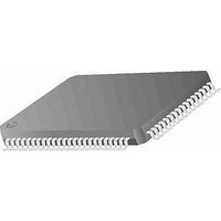
MC9S12E64CFU Freescale Semiconductor, MC9S12E64CFU Datasheet - Page 513

MC9S12E64CFU
Manufacturer Part Number
MC9S12E64CFU
Description
IC MCU 64K FLASH 25MHZ 80-QFP
Manufacturer
Freescale Semiconductor
Series
HCS12r
Specifications of MC9S12E64CFU
Core Processor
HCS12
Core Size
16-Bit
Speed
25MHz
Connectivity
EBI/EMI, I²C, SCI, SPI
Peripherals
POR, PWM, WDT
Number Of I /o
60
Program Memory Size
64KB (64K x 8)
Program Memory Type
FLASH
Ram Size
4K x 8
Voltage - Supply (vcc/vdd)
2.35 V ~ 2.75 V
Data Converters
A/D 16x10b; D/A 2x8b
Oscillator Type
Internal
Operating Temperature
-40°C ~ 85°C
Package / Case
80-QFP
Data Bus Width
16 bit
Data Ram Size
4 KB
Interface Type
SCI, SPI
Maximum Clock Frequency
25 MHz
Number Of Programmable I/os
60
Number Of Timers
16 bit
Maximum Operating Temperature
+ 85 C
Mounting Style
SMD/SMT
Minimum Operating Temperature
- 40 C
On-chip Adc
10 bit
On-chip Dac
8 bit, 2 Channel
For Use With
M68EVB912E128 - BOARD EVAL FOR MC9S12E128/64
Lead Free Status / RoHS Status
Contains lead / RoHS non-compliant
Eeprom Size
-
Lead Free Status / Rohs Status
No RoHS Version Available
Available stocks
Company
Part Number
Manufacturer
Quantity
Price
Company:
Part Number:
MC9S12E64CFU
Manufacturer:
Freescale Semiconductor
Quantity:
10 000
Company:
Part Number:
MC9S12E64CFUE
Manufacturer:
Freescale Semiconductor
Quantity:
10 000
Part Number:
MC9S12E64CFUE
Manufacturer:
FREESCALE
Quantity:
20 000
Company:
Part Number:
MC9S12E64CFUER
Manufacturer:
Freescale Semiconductor
Quantity:
10 000
- Current page: 513 of 606
- Download datasheet (4Mb)
Chapter 18
Multiplexed External Bus Interface (MEBIV3)
18.1
This section describes the functionality of the multiplexed external bus interface (MEBI) sub-block of the
S12 core platform. The functionality of the module is closely coupled with the S12 CPU and the memory
map controller (MMC) sub-blocks.
Figure 18-1
pins that are accessible externally. On some chips, these may not all be bonded out.
The MEBI sub-block of the core serves to provide access and/or visibility to internal core data
manipulation operations including timing reference information at the external boundary of the core and/or
system. Depending upon the system operating mode and the state of bits within the control registers of the
MEBI, the internal 16-bit read and write data operations will be represented in 8-bit or 16-bit accesses
externally. Using control information from other blocks within the system, the MEBI will determine the
appropriate type of data access to be generated.
18.1.1
The block name includes these distinctive features:
Freescale Semiconductor
•
•
•
•
•
•
•
•
•
External bus controller with four 8-bit ports A,B, E, and K
Data and data direction registers for ports A, B, E, and K when used as general-purpose I/O
Control register to enable/disable alternate functions on ports E and K
Mode control register
Control register to enable/disable pull resistors on ports A, B, E, and K
Control register to enable/disable reduced output drive on ports A, B, E, and K
Control register to configure external clock behavior
Control register to configure IRQ pin operation
Logic to capture and synchronize external interrupt pin inputs
Introduction
Features
is a block diagram of the MEBI. In
MC9S12E128 Data Sheet, Rev. 1.07
Figure
18-1, the signals on the right hand side represent
513
Related parts for MC9S12E64CFU
Image
Part Number
Description
Manufacturer
Datasheet
Request
R
Part Number:
Description:
Manufacturer:
Freescale Semiconductor, Inc
Datasheet:
Part Number:
Description:
Manufacturer:
Freescale Semiconductor, Inc
Datasheet:
Part Number:
Description:
Manufacturer:
Freescale Semiconductor, Inc
Datasheet:
Part Number:
Description:
Manufacturer:
Freescale Semiconductor, Inc
Datasheet:
Part Number:
Description:
Manufacturer:
Freescale Semiconductor, Inc
Datasheet:
Part Number:
Description:
Manufacturer:
Freescale Semiconductor, Inc
Datasheet:
Part Number:
Description:
Manufacturer:
Freescale Semiconductor, Inc
Datasheet:
Part Number:
Description:
Manufacturer:
Freescale Semiconductor, Inc
Datasheet:
Part Number:
Description:
Manufacturer:
Freescale Semiconductor, Inc
Datasheet:
Part Number:
Description:
Manufacturer:
Freescale Semiconductor, Inc
Datasheet:
Part Number:
Description:
Manufacturer:
Freescale Semiconductor, Inc
Datasheet:
Part Number:
Description:
Manufacturer:
Freescale Semiconductor, Inc
Datasheet:
Part Number:
Description:
Manufacturer:
Freescale Semiconductor, Inc
Datasheet:
Part Number:
Description:
Manufacturer:
Freescale Semiconductor, Inc
Datasheet:
Part Number:
Description:
Manufacturer:
Freescale Semiconductor, Inc
Datasheet:


