MC9S12E64CFU Freescale Semiconductor, MC9S12E64CFU Datasheet - Page 25
MC9S12E64CFU
Manufacturer Part Number
MC9S12E64CFU
Description
IC MCU 64K FLASH 25MHZ 80-QFP
Manufacturer
Freescale Semiconductor
Series
HCS12r
Specifications of MC9S12E64CFU
Core Processor
HCS12
Core Size
16-Bit
Speed
25MHz
Connectivity
EBI/EMI, I²C, SCI, SPI
Peripherals
POR, PWM, WDT
Number Of I /o
60
Program Memory Size
64KB (64K x 8)
Program Memory Type
FLASH
Ram Size
4K x 8
Voltage - Supply (vcc/vdd)
2.35 V ~ 2.75 V
Data Converters
A/D 16x10b; D/A 2x8b
Oscillator Type
Internal
Operating Temperature
-40°C ~ 85°C
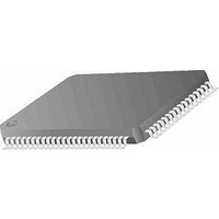
Package / Case
80-QFP
Data Bus Width
16 bit
Data Ram Size
4 KB
Interface Type
SCI, SPI
Maximum Clock Frequency
25 MHz
Number Of Programmable I/os
60
Number Of Timers
16 bit
Maximum Operating Temperature
+ 85 C
Mounting Style
SMD/SMT
Minimum Operating Temperature
- 40 C
On-chip Adc
10 bit
On-chip Dac
8 bit, 2 Channel
For Use With
M68EVB912E128 - BOARD EVAL FOR MC9S12E128/64
Lead Free Status / RoHS Status
Contains lead / RoHS non-compliant
Eeprom Size
-
Lead Free Status / Rohs Status
No RoHS Version Available
Available stocks
Company
Part Number
Manufacturer
Quantity
Price
Company:

Part Number:
MC9S12E64CFU
Manufacturer:
Freescale Semiconductor
Quantity:
10 000
Company:
Part Number:
MC9S12E64CFUE
Manufacturer:
Freescale Semiconductor
Quantity:
10 000
Part Number:
MC9S12E64CFUE
Manufacturer:
FREESCALE
Quantity:
20 000
Company:
Part Number:
MC9S12E64CFUER
Manufacturer:
Freescale Semiconductor
Quantity:
10 000


1.2
Table 1-1
Figure 1-4
Freescale Semiconductor
Device Memory Map
shows the device register map of the MC9S12E128 after reset.
illustrate the device memory map with Flash and RAM.
0x00C8–0x00CF Serial Communications Interface 0 (SCI0)
0x00D8–0x00DF Serial Peripheral Interface (SPI)
0x001A–0x001B
0x001C–0x001F
0x00B0–0x00C7 Reserved
0x00D0–0x00D7 Serial Communications Interface 1 (SCI1)
0x00E0–0x00E7
0x00E8–0x00EF Serial Communications Interface 2 (SCI2)
0x01B0–0x01DF Reserved
0x01E0–0x01FF
0x0080–0x00AF
0x00F0–0x00F3
0x00F4–0x00F7
0x00F8–0x00FF
0x0100- 0x010F
0x0180–0x01AF
0x0280–0x03FF
0x0000–0x0017
0x0020–0x002F
0x0030–0x0033
0x0034–0x003F
0x0040–0x006F
0x0070–0x007F
0x0110–0x013F
0x0140–0x016F
0x0170–0x017F
0x0200–0x023F
0x0240–0x027F
Address
0x0018
0x0019
CORE (Ports A, B, E, Modes, Inits, Test)
Reserved
Voltage Regulator (VREG)
Device ID register (PARTID)
CORE (MEMSIZ, IRQ, HPRIO)
CORE (DBG)
CORE (PPAGE, Port K)
Clock and Reset Generator (PLL, RTI, COP)
Standard Timer 16-bit 4 channels (TIM0)
Reserved
Analog to Digital Converter 10-bit 16 channels (ATD)
Inter IC Bus
Digital to Analog Converter 8-bit 1-channel (DAC0)
Digital to Analog Converter 8-bit 1-channel (DAC1)
Reserved
Flash Control Register
Reserved
Standard Timer 16-bit 4 channels (TIM1)
Reserved
Standard Timer 16-bit 4 channels (TIM2)
Pulse Width Modulator 8-bit 6 channels (PWM)
Pulse Width Modulator with Fault 15-bit 6 channels (PMF)
Port Integration Module (PIM)
Reserved
Table 1-1. Device Register Map Overview
MC9S12E128 Data Sheet, Rev. 1.07
Module
Chapter 1 MC9S12E128 Device Overview (MC9S12E128DGV1)
Figure
1-2,
Size
384
24
16
12
48
16
48
24
16
48
48
16
48
48
32
64
64
1
8
Figure 1-3
1
2
4
4
8
8
8
8
8
4
4
and
25
Related parts for MC9S12E64CFU
Image
Part Number
Description
Manufacturer
Datasheet
Request
R

Part Number:
Description:
Manufacturer:
Freescale Semiconductor, Inc
Datasheet:
Part Number:
Description:
Manufacturer:
Freescale Semiconductor, Inc
Datasheet:
Part Number:
Description:
Manufacturer:
Freescale Semiconductor, Inc
Datasheet:
Part Number:
Description:
Manufacturer:
Freescale Semiconductor, Inc
Datasheet:
Part Number:
Description:
Manufacturer:
Freescale Semiconductor, Inc
Datasheet:
Part Number:
Description:
Manufacturer:
Freescale Semiconductor, Inc
Datasheet:
Part Number:
Description:
Manufacturer:
Freescale Semiconductor, Inc
Datasheet:
Part Number:
Description:
Manufacturer:
Freescale Semiconductor, Inc
Datasheet:
Part Number:
Description:
Manufacturer:
Freescale Semiconductor, Inc
Datasheet:
Part Number:
Description:
Manufacturer:
Freescale Semiconductor, Inc
Datasheet:
Part Number:
Description:
Manufacturer:
Freescale Semiconductor, Inc
Datasheet:
Part Number:
Description:
Manufacturer:
Freescale Semiconductor, Inc
Datasheet:
Part Number:
Description:
Manufacturer:
Freescale Semiconductor, Inc
Datasheet:
Part Number:
Description:
Manufacturer:
Freescale Semiconductor, Inc
Datasheet:
Part Number:
Description:
Manufacturer:
Freescale Semiconductor, Inc
Datasheet: