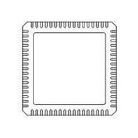
71M6531F-IM/F Maxim Integrated Products, 71M6531F-IM/F Datasheet - Page 114

71M6531F-IM/F
Manufacturer Part Number
71M6531F-IM/F
Description
IC ENERGY METER 256KB 68-QFN
Manufacturer
Maxim Integrated Products
Datasheet
1.71M6531D-IMRF.pdf
(120 pages)
Specifications of 71M6531F-IM/F
Mounting Style
SMD/SMT
Package / Case
QFN-68
Lead Free Status / RoHS Status
Lead free / RoHS Compliant
- Current page: 114 of 120
- Download datasheet (3Mb)
Data Sheet 71M6531D/F-71M6532D/F
5.9.3
1)
114
COM3,COM2,
COM1,COM0
SEG0…SEG2,
SEG7, SEG8
SEG12…SEG18
SEG20…SEG23
SEG24/DIO4…
SEG35/DIO15,
SEG37/DIO17,
SEG48/DIO28,
SEG49/DIO29,
SEG63/DIO43…
SEG66/DIO46
SEG3/PCLK
SEG4/PSDO
SEG5/PCSZ
SEG6/PSDI
E_RXTX/SEG9
E_RST/SEG11
E_TCLK/SEG10
ICE_E
CKTEST/SEG19,
MUXSYNC/SEG7
TMUXOUT
OPT_RX/DIO1
OPT_TX/DIO2
RESET
RX
TX
TEST
PB
Name
Not all pins available on the 71M6531D/F or 71M6532D/F.
Digital Pins
Type Circuit
I/O
I/O
I/O
I/O
I/O
I/O
O
O
O
O
O
O
O
I
I
I
I
I
© 2005-2010 TERIDIAN Semiconductor Corporation
3, 4, 5
3, 4, 5 Multi-use pins, configurable as either LCD SEG driver or SPI PORT.
1, 4, 5
1, 4, 5
3, 4, 7
4, 5
4, 5
3, 4
5
5
5
2
4
2
3
4
7
3
LCD Common Outputs: These 4 pins provide the select signals for
the LCD display.
Dedicated LCD Segment Output pins.
Dedicated LCD Segment Output pins (71M6532D/F only).
Multi-use pins, configurable as either LCD SEG driver or DIO.
(DIO4 = SCK, DIO5 = SDA when configured as EEPROM interface;
WPULSE = DIO6, VARPULSE = DIO7 when configured as pulse
outputs). Unused pins must be configured as outputs or terminated
to V3P3/GNDD.
Multi-use pins, configurable as either emulator port pins (when ICE_E
pulled high) or LCD SEG drivers (when ICE_E tied to GND).
ICE enable. When zero, E_RST, E_TCLK and E_RXTX become
SEG32, SEG33 and SEG38 respectively. For production units, this
pin should be pulled to GND to disable the emulator port.
Multi-use pins, configurable as either multiplexer/clock output or LCD
segment driver using the I/O RAM registers CKOUT_E or
MUX_SYNC_E.
Digital output test multiplexer. Controlled by TMUX[3:0].
Multi-use pin, configurable as Optical Receive Input or general DIO.
When configured as OPT_RX, this pin receives a signal from an external
photo-detector used in an IR serial interface. If this pin is unused it
must be configured as an output or terminated to V3P3D or GNDD.
Multi-use pin, configurable as either optical LED transmit output,
WPULSE, RPULSE, or general DIO. When configured as OPT_TX,
this pin is capable of directly driving an LED for transmitting data in
an IR serial interface.
Chip reset: This input pin is used to reset the chip into a known state.
For normal operation, this pin is pulled low. To reset the chip, this pin
should be pulled high. This pin has an internal 30 μA (nominal) current
source pull-down. No external reset circuitry is necessary.
UART input. If this pin is unused it must be configured as an
output or terminated to V3P3D or GNDD.
UART output.
Enables Production Test. This pin must be grounded in normal
operation.
Push button input. This pin must be at GNDD when not active. A
rising edge sets the IE_PB flag. It also causes the part to wake up if it
is in SLEEP or LCD mode. PB does not have an internal pull-up or
pull-down.
Table 92: Digital Pins
1)
Description
FDS 6531/6532 005
v1.3
Related parts for 71M6531F-IM/F
Image
Part Number
Description
Manufacturer
Datasheet
Request
R

Part Number:
Description:
IC ENERGY METER 256KB 68-QFN
Manufacturer:
Maxim Integrated Products

Part Number:
Description:
MAX7528KCWPMaxim Integrated Products [CMOS Dual 8-Bit Buffered Multiplying DACs]
Manufacturer:
Maxim Integrated Products
Datasheet:

Part Number:
Description:
Single +5V, fully integrated, 1.25Gbps laser diode driver.
Manufacturer:
Maxim Integrated Products
Datasheet:

Part Number:
Description:
Single +5V, fully integrated, 155Mbps laser diode driver.
Manufacturer:
Maxim Integrated Products
Datasheet:

Part Number:
Description:
VRD11/VRD10, K8 Rev F 2/3/4-Phase PWM Controllers with Integrated Dual MOSFET Drivers
Manufacturer:
Maxim Integrated Products
Datasheet:

Part Number:
Description:
Highly Integrated Level 2 SMBus Battery Chargers
Manufacturer:
Maxim Integrated Products
Datasheet:

Part Number:
Description:
Current Monitor and Accumulator with Integrated Sense Resistor; ; Temperature Range: -40°C to +85°C
Manufacturer:
Maxim Integrated Products

Part Number:
Description:
TSSOP 14/A�/RS-485 Transceivers with Integrated 100O/120O Termination Resis
Manufacturer:
Maxim Integrated Products

Part Number:
Description:
TSSOP 14/A�/RS-485 Transceivers with Integrated 100O/120O Termination Resis
Manufacturer:
Maxim Integrated Products

Part Number:
Description:
QFN 16/A�/AC-DC and DC-DC Peak-Current-Mode Converters with Integrated Step
Manufacturer:
Maxim Integrated Products

Part Number:
Description:
TDFN/A/65V, 1A, 600KHZ, SYNCHRONOUS STEP-DOWN REGULATOR WITH INTEGRATED SWI
Manufacturer:
Maxim Integrated Products

Part Number:
Description:
Integrated Temperature Controller f
Manufacturer:
Maxim Integrated Products

Part Number:
Description:
SOT23-6/I�/45MHz to 650MHz, Integrated IF VCOs with Differential Output
Manufacturer:
Maxim Integrated Products

Part Number:
Description:
SOT23-6/I�/45MHz to 650MHz, Integrated IF VCOs with Differential Output
Manufacturer:
Maxim Integrated Products

Part Number:
Description:
EVALUATION KIT/2.4GHZ TO 2.5GHZ 802.11G/B RF TRANSCEIVER WITH INTEGRATED PA
Manufacturer:
Maxim Integrated Products


