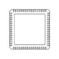
71M6531F-IM/F Maxim Integrated Products, 71M6531F-IM/F Datasheet - Page 81

71M6531F-IM/F
Manufacturer Part Number
71M6531F-IM/F
Description
IC ENERGY METER 256KB 68-QFN
Manufacturer
Maxim Integrated Products
Datasheet
1.71M6531D-IMRF.pdf
(120 pages)
Specifications of 71M6531F-IM/F
Mounting Style
SMD/SMT
Package / Case
QFN-68
Lead Free Status / RoHS Status
Lead free / RoHS Compliant
- Current page: 81 of 120
- Download datasheet (3Mb)
FDS 6531/6532 005
v1.3
IEN_WD_NROVF 20B0[0]
IE_XFER
IE_RTC
IE_WAKE
INTBITS
LCD_BITMAP
[31:24]
LCD_BITMAP
[39:32]
LCD_BITMAP
[55:48]
LCD_BITMAP
[63:56]
LCD_BITMAP
[71:64]
LCD_BLKMAP19
[3:0]
LCD_BLKMAP18
[3:0]
LCD_CLK[1:0]
Name
SFR E8[0]
SFR E8[1]
SFR E8[5]
SFR F8[6:0]
2023
2024
2026
2027
2028
205A[7:4]
205A[3:0]
2021[1:0]
Location
Reset
0
0
0
0
–
0
0
0
0
0
0
0
Wake
0
0
0
–
–
L
L
L
L
L
L
L
© 2005-2010 TERIDIAN Semiconductor Corporation
R/W
R/W
R/W
R/W
R/W
R/W
R/W
R/W
R/W
R/W
R/W
Dir
Active high watchdog near overflow interrupt enable.
Interrupt flags. These flags monitor the XFER_BUSY interrupt and the RTC_1SEC
interrupt. The flags are set by hardware and clear automatically.
Indicates that the MPU was awakened by the autowake timer. This bit is typically read
by the MPU on bootup. The firmware must write a zero to this bit to clear it.
Interrupt inputs. The MPU may read these bits to see the status of external interrupts
INT0, INT1 up to INT6. These bits do not have any memory and are primarily intended
for debug use.
Configuration for DIO11/SEG31 through DIO4/SEG24. Unused bits should be set to zero.
Bitmap of DIO19/SEG39 through DIO12/SEG32. Unused bits should be set to zero.
Bitmap of DIO28/SEG48 through DIO35/SEG55. Unused bits should be set to zero.
Bitmap of DIO36/SEG56 through DIO43/SEG63. Unused bits should be set to zero.
Bitmap of DIO44/SEG64 through DIO51/SEG71. Unused bits should be set to zero.
Identifies which segments connected to SEG18 and SEG19 should blink. 1 means
blink. The most significant bit corresponds to COM3, the least significant bit to COM0.
Sets the LCD clock frequency for COM/SEG pins (not
following (f
1 = LCD pin, 0 = DIO pin. Check
1 = LCD pin, 0 = DIO pin. Check
1 = LCD pin, 0 = DIO pin. Check
1 = LCD pin, 0 = DIO pin. Check
1 = LCD pin, 0 = DIO pin. Check
00 = f
01 = f
10 = f
11 = f
w
w/
w
w
w
/2
/2
/2
2
= 32768 Hz):
8
9
7
6
Table 54
Table 54
Table 54
Table 54
Table 54
Description
for bit availability.
for bit availability.
for bit availability.
for bit availability.
for bit availability.
Data Sheet 71M6531D/F-71M6532D/F
frame rate) according to the
81
Related parts for 71M6531F-IM/F
Image
Part Number
Description
Manufacturer
Datasheet
Request
R

Part Number:
Description:
IC ENERGY METER 256KB 68-QFN
Manufacturer:
Maxim Integrated Products

Part Number:
Description:
MAX7528KCWPMaxim Integrated Products [CMOS Dual 8-Bit Buffered Multiplying DACs]
Manufacturer:
Maxim Integrated Products
Datasheet:

Part Number:
Description:
Single +5V, fully integrated, 1.25Gbps laser diode driver.
Manufacturer:
Maxim Integrated Products
Datasheet:

Part Number:
Description:
Single +5V, fully integrated, 155Mbps laser diode driver.
Manufacturer:
Maxim Integrated Products
Datasheet:

Part Number:
Description:
VRD11/VRD10, K8 Rev F 2/3/4-Phase PWM Controllers with Integrated Dual MOSFET Drivers
Manufacturer:
Maxim Integrated Products
Datasheet:

Part Number:
Description:
Highly Integrated Level 2 SMBus Battery Chargers
Manufacturer:
Maxim Integrated Products
Datasheet:

Part Number:
Description:
Current Monitor and Accumulator with Integrated Sense Resistor; ; Temperature Range: -40°C to +85°C
Manufacturer:
Maxim Integrated Products

Part Number:
Description:
TSSOP 14/A�/RS-485 Transceivers with Integrated 100O/120O Termination Resis
Manufacturer:
Maxim Integrated Products

Part Number:
Description:
TSSOP 14/A�/RS-485 Transceivers with Integrated 100O/120O Termination Resis
Manufacturer:
Maxim Integrated Products

Part Number:
Description:
QFN 16/A�/AC-DC and DC-DC Peak-Current-Mode Converters with Integrated Step
Manufacturer:
Maxim Integrated Products

Part Number:
Description:
TDFN/A/65V, 1A, 600KHZ, SYNCHRONOUS STEP-DOWN REGULATOR WITH INTEGRATED SWI
Manufacturer:
Maxim Integrated Products

Part Number:
Description:
Integrated Temperature Controller f
Manufacturer:
Maxim Integrated Products

Part Number:
Description:
SOT23-6/I�/45MHz to 650MHz, Integrated IF VCOs with Differential Output
Manufacturer:
Maxim Integrated Products

Part Number:
Description:
SOT23-6/I�/45MHz to 650MHz, Integrated IF VCOs with Differential Output
Manufacturer:
Maxim Integrated Products

Part Number:
Description:
EVALUATION KIT/2.4GHZ TO 2.5GHZ 802.11G/B RF TRANSCEIVER WITH INTEGRATED PA
Manufacturer:
Maxim Integrated Products


