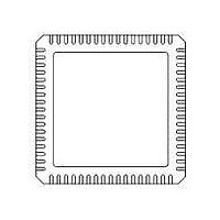
71M6531F-IM/F Maxim Integrated Products, 71M6531F-IM/F Datasheet - Page 15

71M6531F-IM/F
Manufacturer Part Number
71M6531F-IM/F
Description
IC ENERGY METER 256KB 68-QFN
Manufacturer
Maxim Integrated Products
Datasheet
1.71M6531D-IMRF.pdf
(120 pages)
Specifications of 71M6531F-IM/F
Mounting Style
SMD/SMT
Package / Case
QFN-68
Lead Free Status / RoHS Status
Lead free / RoHS Compliant
•
•
•
•
•
The CE program resides in flash memory. Common access to flash memory by CE and MPU is controlled
by a memory share circuit. Each CE instruction word is two bytes long. Allocated flash space for the CE
program cannot exceed 4096 16-bit words (8 KB). The CE program counter begins a pass through the
CE code each time multiplexer state 0 begins. The code pass ends when a HALT instruction is executed.
For proper operation, the code pass must be completed before the multiplexer cycle ends (see Section
2.2 System Timing
The CE program must begin on a 1-KB boundary of the flash address. The I/O RAM register CE_LCTN[7:0]
defines which 1-KB boundary contains the CE code. Thus, the first CE instruction is located at
1024*CE_LCTN[7:0].
The CE can access up to 4 KB of data RAM (XRAM), or 1024 32-bit data words, starting at RAM address
0x0000.
The XRAM can be accessed by the FIR filter block, the RTM circuit, the CE, and the MPU. Assigned time
slots are reserved for FIR, and MPU, respectively, to prevent bus contention for XRAM data access.
The MPU can read and write the XRAM as the primary means of data communication between the two
processors.
DIO_PV and DIO_PW (pulse count assist) bits and PRE_SAMPS[1:0] and SUM_CYCLES[5:0] (accumulation
assist).
PRE_SAMPS[1:0] and SUM_CYCLES[5:0] support a dual level accumulation scheme where the first
accumulator accumulates results from PRE_SAMPS[1:0] samples and the second accumulator accumulates
up to SUM_CYCLES[5:0] of the first accumulator results. The integration time for each energy output is
PRE_SAMPS[1:0] * SUM_CYCLES[5:0]/2520.6 (with MUX_DIV[3:0] = 1). The CE hardware issues the
XFER_BUSY interrupt when the accumulation is complete.
FDS 6531/6532 005
1.3
The CE, a dedicated 32-bit signal processor, performs the precision computations necessary to accurately
measure energy. The CE calculations and processes include:
•
•
•
The CE is aided by support hardware to facilitate implementation of equations, pulse counters and
accumulators. This hardware is controlled through I/O RAM locations EQU[2:0] (equation assist), the
v1.3
Multiplication of each current sample with its associated voltage sample to obtain the energy per
sample (when multiplied with the constant sample time).
Frequency-insensitive delay cancellation on all four channels (to compensate for the delay between
samples caused by the multiplexing scheme).
90° phase shifter (for VAR calculations).
Pulse generation.
Monitoring of the input signal frequency (for frequency and phase information).
Monitoring of the input signal amplitude (for sag detection).
Scaling of the processed samples based on calibration coefficients.
Scaling of all samples based on temperature compensation information (71M6532D/F only).
Digital Computation Engine (CE)
Table
4 shows the CE addresses in XRAM allocated to analog inputs from the AFE.
Summary).
© 2005-2010 TERIDIAN Semiconductor Corporation
Address (HEX)
Table 4: XRAM Locations for ADC Results
0x04...0x09
0x0A
0x0B
0x00
0x01
0x02
0x03
Name
TEMP
VBAT
VA
VB
IA
IB
–
Phase A voltage
Phase B voltage
Phase A current
Phase B current
Battery Voltage
Temperature
Description
Not used
Data Sheet 71M6531D/F-71M6532D/F
15


