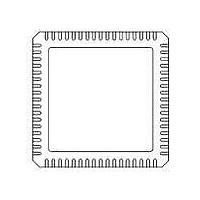
71M6531F-IM/F Maxim Integrated Products, 71M6531F-IM/F Datasheet - Page 39

71M6531F-IM/F
Manufacturer Part Number
71M6531F-IM/F
Description
IC ENERGY METER 256KB 68-QFN
Manufacturer
Maxim Integrated Products
Datasheet
1.71M6531D-IMRF.pdf
(120 pages)
Specifications of 71M6531F-IM/F
Mounting Style
SMD/SMT
Package / Case
QFN-68
Lead Free Status / RoHS Status
Lead free / RoHS Compliant
failure can be detected with the FWCOL0 or FWCOL1 interrupt and the write can be retried.
It is practical to pre-erase pages, disable interrupts and poll the CE_BUSY interrupt flag, IRCON[2]. This
method avoids problems with interrupt latency, but can still result in a write failure if the CE code takes to
much time. As mentioned above, polling FWCOL0 and FWCOL1 can detect write failures. However, the
speed in a polling write is only 2520 bytes per second and the firmware cannot respond to interrupts.
As an alternative to using flash, a small EEPROM can store data without compromises. EEPROM interfaces
are included in the device.
The original state of a flash byte is 0xFF (all ones). Once a value other than 0xFF is written to a flash
memory cell, overwriting with a different value usually requires that the cell be erased first. Since cells
cannot be erased individually, the page has to be copied to RAM, followed by a page erase. After this,
the page can be updated in RAM and then written back to the flash memory.
2. Write pattern 0xAA to FLSH_ERASE (SFR 0x94).
The page erase sequence is:
1. Write the page address to FLSH_PGADR[5:0] (SFR 0xB7[7:1]).
2. Write pattern 0x55 to FLSH_ERASE (SFR 0x94).
The program memory of the 71M6531 consists of a fixed lower bank of 32 KB addressable at 0x0000 to
0x7FFF plus an upper bank area of 32 KB, addressable at 0x8000 to 0xFFFF. The upper 32 KB space is
banked using the I/O RAM FL_BANK register as follows:
•
Table 38 illustrates the bank switching mechanism.
FDS 6531/6532 005
The simplest flash write procedure disables the CE during the write operation and interpolates the metering
measurements. However, this results in the loss of at least one second of data, because the CE has to
resynchronize with the mains voltage.
There is a brief guaranteed interval (typically 1/32768 s) between CE executions which occurs 2520 times
per second. The start of the interval can be detected with the CE_BUSY interrupt which occurs on the
falling edge of CE_BUSY (an internal signal measurable from TMUXOUT). However, this guaranteed idle
time (30.5 µs) is too short to write a byte which takes 42 µs or to erase a page of flash memory which
takes at least 20 ms. Some CE code has substantially longer idle times, but in those cases, firmware
interrupt latencies can easily consume the available write time. If a flash write fails in this scheme, the
Updating Individual Bytes in Flash Memory
Flash Erase Procedures
Flash erasure is initiated by writing a specific data pattern to specific SFR registers in the proper sequence.
These special pattern/sequence requirements prevent inadvertent erasure of the flash memory.
The mass erase sequence is:
1. Write 1 to the FLSH_MEEN bit (SFR 0xB2[1]).
Bank-Switching:
•
v1.3
The 71M6531D provides 4 banks of 32 KB each selected by FL_BANK[1:0]. Note that when
FL_BANK[1:0] = 00, the upper bank is the same as the lower bank.
The 71M6531F and 71M6532D/F provide 8 banks of 32 KB each selected by FL_BANK[2:0].
The mass erase cycle can only be initiated when the ICE port is enabled.
© 2005-2010 TERIDIAN Semiconductor Corporation
Data Sheet 71M6531D/F-71M6532D/F
39


