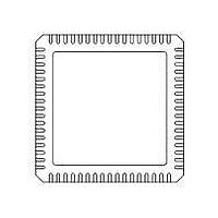
71M6531F-IM/F Maxim Integrated Products, 71M6531F-IM/F Datasheet - Page 17

71M6531F-IM/F
Manufacturer Part Number
71M6531F-IM/F
Description
IC ENERGY METER 256KB 68-QFN
Manufacturer
Maxim Integrated Products
Datasheet
1.71M6531D-IMRF.pdf
(120 pages)
Specifications of 71M6531F-IM/F
Mounting Style
SMD/SMT
Package / Case
QFN-68
Lead Free Status / RoHS Status
Lead free / RoHS Compliant
5 updates per MUX interval and if the MUX interval is 1950 cycles long, the ideal value for the interval is
1950/5/4 = 97.5. If PLS_INTERVAL = 98, the fifth output will occur too late and be lost. In this case, the
proper value for PLS_INTERVAL is 97.
PLS_MAXWIDTH = 255, no width checking is performed.
The WPULSE and RPULSE pulse generator outputs are available on DIO6 and DIO7, respectively. They
can also be output on OPT_TX (see OPT_TXE[1:0] for details).
1024 32-bit words, shared between the CE and the MPU using a time-multiplex method. This reduces
MPU wait states when accessing CE data. When the MPU and CE are clocking at maximum frequency
(10 MHz), the DRAM will make up to four accesses during each 100 ns interval. These consist of two
MPU accesses, one CE access and one SPI access.
The Data RAM is 32 bits wide and uses an external multiplexer so as to appear byte-wide to the MPU.
The Data RAM hardware will convert an MPU byte write operation into a read-modify-write operation that
requires two Data RAM accesses. The second access is guaranteed to be available because the MPU
cannot access the XRAM on two consecutive instructions unless it is using the same address.
In addition to the reduction of wait states, this arrangement permits the MPU to easily use unneeded CE
data memory. Likewise, the amount of memory the CE uses is not limited by the size of a dedicated CE
data RAM.
In traditional meter ICs, sampling is accomplished by using two A/D converters per phase (one for voltage
and the other one for current) controlled to sample simultaneously. Teridian’s patented Single-Converter
Technology
and the corresponding current samples that are obtained with a single multiplexed A/D converter.
The “constant delay” all-pass filters provide a broad-band delay β, that is precisely matched to the differ-
ence in sample time between the voltage and the current of a given phase. This digital filter does not af-
fect the amplitude of the signal, but provides a precisely controlled phase response. The delay compen-
sation implemented in the CE aligns the voltage samples with their corresponding current samples by
routing the voltage samples through the all-pass filter, thus delaying the voltage samples by β, resulting in
the residual phase error β – Ф. The residual phase error is negligible, and is typically less than ±1.5 milli-
degrees at 100Hz, thus it does not contribute to errors in the energy measurements.
samples taken during one multiplexer cycle.
The number of samples processed during one accumulation cycle is controlled by PRE_SAMPS[1:0]
(IORAM 0x2001[7:6]) and SUM_CYCLES[5:0] (IORAM 0x2001[5:0]). The integration time for each energy
output is:
FDS 6531/6532 005
Since the FIFO resets at the beginning of each MUX frame, the user must specify PLS_INTERVAL so that
all of the pulse updates are output before
Hardware also provides a maximum pulse width feature. The PLS_MAXWIDTH register selects a maximum
negative pulse width to be Nmax updates according to the formula: Nmax = (2*PLS_MAXWIDTH+1). If
1.3.4
The CE and MPU use a single general-purpose Data RAM (also referred to as XRAM). The Data RAM is
1.3.5
When measuring the energy of a phase (i.e., Wh and VARh) in a service, the voltage and current for that
phase must be sampled at the same instant. Otherwise, the phase difference, Ф, introduces errors.
Where f is the frequency of the input signal and t
delay” all-pass filters. These all-pass filters correct for the conversion time difference between the voltage
1.3.6
The ADC processes one sample per channel per multiplexer cycle.
v1.3
Delay Compensation
CE Functional Overview
PRE_SAMPS[1:0] * SUM_CYCLES[5:0] / 2520.6, where 2520.6 is the sample rate [Hz]
Data RAM (XRAM)
®
, however, exploits the 32-bit signal processing capability of its CE to implement “constant
φ
=
t
delay
T
© 2005-2010 TERIDIAN Semiconductor Corporation
⋅
360
o
=
t
delay
⋅
the MUX frame completes. For instance, if the CE code outputs
f
⋅
360
o
delay
is the sampling delay between voltage and current.
Data Sheet 71M6531D/F-71M6532D/F
Figure 6
shows the timing of the
17


