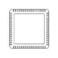
71M6531F-IM/F Maxim Integrated Products, 71M6531F-IM/F Datasheet - Page 37

71M6531F-IM/F
Manufacturer Part Number
71M6531F-IM/F
Description
IC ENERGY METER 256KB 68-QFN
Manufacturer
Maxim Integrated Products
Datasheet
1.71M6531D-IMRF.pdf
(120 pages)
Specifications of 71M6531F-IM/F
Mounting Style
SMD/SMT
Package / Case
QFN-68
Lead Free Status / RoHS Status
Lead free / RoHS Compliant
this feature may disturb the ADC, it is recommended that this option be avoided when possible.
The MPU clock frequency CKMPU is determined by another divider controlled by the I/O RAM field
MPU_DIV[2:0] and can be set to MCK/2
also generates the 2 x CKMPU clock for use by the emulator. The emulator clock is not generated when
ECK_DIS is asserted.
During a power-on reset, [M40MHZ, M26MHZ] defaults to [0,0] and the MCK divider is set to divide by 4.
When [M40MHZ, M26MHZ] = [1,0], the CE clock frequency may be set to ~5 MHz (4.9152 MHz) or ~10
MHz (9.8304 MHz), using the I/O RAM register CE10MHZ. In this mode, the ADC and FIR clock frequen-
cies remain at ~ 5 MHz. When [M40MHZ, M26MHZ] = [0,1], the CE, ADC, FIR and MPU clock frequen-
cies are shifted to ~ 6.6 MHz (6.5536 MHz). This increases the ADC sample rate by 33%.
In sleep mode, the M40MHZ and M26MHZ inputs to the clock generator are forced low. In brownout
mode, the clocks are derived from the crystal oscillator and the clock frequencies are scaled by 7/8.
supply). The RTC consists of a counter chain and output registers. The counter chain consists of registers
for seconds, minutes, hours, day of week, day of month, month and year. The RTC is capable of
processing leap years. Each counter has its own output register. Whenever the MPU reads the seconds
register, all other output registers are automatically updated. Since the RTC clock (RTCLK) is not coherent
to the MPU clock, the MPU must read the seconds register until two consecutive reads are the same (this
requires either 2 or 3 reads). At this point, all RTC output registers will have the correct time. Regardless
of the MPU clock speed, RTC reads require one wait state.
RTC time is set by writing to the registers RTC_SEC[5:0] through RTC_YR. Each write operation must be
preceded by a write operation to the WE register in I/O RAM. The value written to the WE register is
unimportant.
Time adjustments are written to the RTCA_ADJ[6:0], PREG[16:0] and QREG[1:0] registers. Updates to
PREG[16:0] and QREG[1:0] must occur after the one second interrupt and must be finished before reaching
the next one second boundary. The new values are loaded into the counters at the next one second
boundary.
PREG[16:0] and QREG[1:0] are separate registers in the device hardware, but the bits are 16-bit contiguous
so the MPU firmware can treat them as a single register. A single binary number can be calculated and
then loaded into them at the same time.
The 71M6531D/F and 71M6532D/F have two rate adjustment mechanisms. The first is an analog rate
adjustment, using RTCA_ADJ[6:0], which trims the crystal load capacitance. Setting RTCA_ADJ[6:0] to 00
minimizes the load capacitance, maximizing the oscillator frequency. Setting RTCA_ADJ[6:0] to 0x3F
maximizes the load capacitance, minimizing the oscillator frequency. The adjustable capacitance is
approximately:
will depend on the crystal properties. The adjustment may occur at any time and the resulting clock
frequency can be measured over a one-second interval.
The second rate adjustment is a digital rate adjust using PREG[16:0] and QREG[1:0], which can be used
to adjust the clock rate up to ± 988 ppm, with a resolution of 3.8 ppm. Updates must occur after a one
second interrupt and must finish before the next one second boundary. The rate adjustment will be
implemented starting at the next one second boundary. Since the LSB results in an adjustment every
four seconds, the frequency should be measured over an interval that is a multiple of four seconds.
FDS 6531/6532 005
The PLL generates a 2x emulator clock which is controlled by the ECK_DIS bit. Since clock noise from
1.5.3
The RTC is driven directly by the crystal oscillator. It is powered by the net RTC_NV (battery-backed up
The maximum adjustment range is approximately-12 ppm to +22ppm. The precise amount of adjustment
v1.3
Real-Time Clock (RTC)
particular CE code may render it unusable.
CE codes are tailored to particular clock frequencies. Changing the clock frequency for a
© 2005-2010 TERIDIAN Semiconductor Corporation
C
ADJ
( MPU_DIV +2)
=
RTCA
Hz where MPU_DIV[2:0] varies from 0 to 6. The circuit
128
_
ADJ
⋅
16
5 .
pF
Data Sheet 71M6531D/F-71M6532D/F
37


