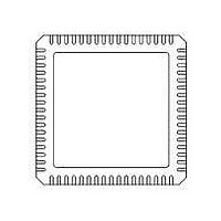
71M6531F-IM/F Maxim Integrated Products, 71M6531F-IM/F Datasheet - Page 14

71M6531F-IM/F
Manufacturer Part Number
71M6531F-IM/F
Description
IC ENERGY METER 256KB 68-QFN
Manufacturer
Maxim Integrated Products
Datasheet
1.71M6531D-IMRF.pdf
(120 pages)
Specifications of 71M6531F-IM/F
Mounting Style
SMD/SMT
Package / Case
QFN-68
Lead Free Status / RoHS Status
Lead free / RoHS Compliant
- Current page: 14 of 120
- Download datasheet (3Mb)
an accumulation interval and CROSS always toggles near the end of each multiplexer frame.
The internal bias voltage, VBIAS (typically 1.6 V), is used by the ADC when measuring the temperature
and battery monitor signals.
reference. It is used to determine the die temperature. The MPU may request an alternate multiplexer
cycle containing the temperature sensor output by asserting MUX_ALT.
The primary use of the temperature data is to determine the magnitude of compensation required to offset
the thermal drift in the system (see Section
the battery and a scaled fraction of the battery voltage is applied to the ADC input. After each alternative
MUX frame, the result of the ADC conversion is available at XRAM address 0x0B. BME is ignored and
assumed zero when system power is not available (V1 < VBIAS). See Section
VB) are sampled, and the ADC counts obtained are stored in XRAM where they can be accessed by the
CE and, if necessary, by the MPU. Alternate multiplexer cycles are initiated less frequently by the MPU to
gather access to the slow temperature and battery signals.
Figure
(for the 71M6531D/F, the current input for phase A is a single pin [IA]).
Data Sheet 71M6531D/F-71M6532D/F
the number of multiplexer frames in an accumulation interval is always even. Operation with
CHOP_E[1:0] = 00 does not require control of the chopping mechanism by the MPU while eliminating the
offset for temperature measurement.
In the second toggle state, CHOP_E[1:0] = 11, no ALT frame is forced during the last multiplexer cycle in
1.2.6
The 71M6531D/F and 71M6532D/F include an on-chip temperature sensor implemented as a bandgap
1.2.7
The battery voltage is measured by the ADC during alternative multiplexer frames if the BME (Battery
Measure Enable) bit in the I/O RAM is set. While BME is set, an on-chip 45 kΩ load resistor is applied to
1.2.8
The AFE functions as a data acquisition system, controlled by the MPU. The main signals (IA, VA, IB and
14
5 shows the block diagram of the AFE, with current inputs shown only as differential pair of pins
Temperature Sensor
Battery Monitor
AFE Functional Description
Figure 5: AFE Block Diagram (Shown for the 71M6532D/F)
IAP
IAN
© 2005-2010 TERIDIAN Semiconductor Corporation
IBP
IBN
VA
VB
VBAT
SENSOR
TEMP
EQU
MUX_ALT
MUX_DIV
MUX
3.4 Temperature
VREF_CAL
VREF_DIS
VBIAS
VREF
VADC
VREF
Compensation).
CONVERTER
VREF
VBIAS
ADC_E
∆Σ ADC
FIR_LEN
FIR
22
5.4.4 Battery
FDS 6531/6532 005
Monitor.
v1.3
Related parts for 71M6531F-IM/F
Image
Part Number
Description
Manufacturer
Datasheet
Request
R

Part Number:
Description:
IC ENERGY METER 256KB 68-QFN
Manufacturer:
Maxim Integrated Products

Part Number:
Description:
MAX7528KCWPMaxim Integrated Products [CMOS Dual 8-Bit Buffered Multiplying DACs]
Manufacturer:
Maxim Integrated Products
Datasheet:

Part Number:
Description:
Single +5V, fully integrated, 1.25Gbps laser diode driver.
Manufacturer:
Maxim Integrated Products
Datasheet:

Part Number:
Description:
Single +5V, fully integrated, 155Mbps laser diode driver.
Manufacturer:
Maxim Integrated Products
Datasheet:

Part Number:
Description:
VRD11/VRD10, K8 Rev F 2/3/4-Phase PWM Controllers with Integrated Dual MOSFET Drivers
Manufacturer:
Maxim Integrated Products
Datasheet:

Part Number:
Description:
Highly Integrated Level 2 SMBus Battery Chargers
Manufacturer:
Maxim Integrated Products
Datasheet:

Part Number:
Description:
Current Monitor and Accumulator with Integrated Sense Resistor; ; Temperature Range: -40°C to +85°C
Manufacturer:
Maxim Integrated Products

Part Number:
Description:
TSSOP 14/A�/RS-485 Transceivers with Integrated 100O/120O Termination Resis
Manufacturer:
Maxim Integrated Products

Part Number:
Description:
TSSOP 14/A�/RS-485 Transceivers with Integrated 100O/120O Termination Resis
Manufacturer:
Maxim Integrated Products

Part Number:
Description:
QFN 16/A�/AC-DC and DC-DC Peak-Current-Mode Converters with Integrated Step
Manufacturer:
Maxim Integrated Products

Part Number:
Description:
TDFN/A/65V, 1A, 600KHZ, SYNCHRONOUS STEP-DOWN REGULATOR WITH INTEGRATED SWI
Manufacturer:
Maxim Integrated Products

Part Number:
Description:
Integrated Temperature Controller f
Manufacturer:
Maxim Integrated Products

Part Number:
Description:
SOT23-6/I�/45MHz to 650MHz, Integrated IF VCOs with Differential Output
Manufacturer:
Maxim Integrated Products

Part Number:
Description:
SOT23-6/I�/45MHz to 650MHz, Integrated IF VCOs with Differential Output
Manufacturer:
Maxim Integrated Products

Part Number:
Description:
EVALUATION KIT/2.4GHZ TO 2.5GHZ 802.11G/B RF TRANSCEIVER WITH INTEGRATED PA
Manufacturer:
Maxim Integrated Products


