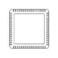
71M6531F-IM/F Maxim Integrated Products, 71M6531F-IM/F Datasheet - Page 80

71M6531F-IM/F
Manufacturer Part Number
71M6531F-IM/F
Description
IC ENERGY METER 256KB 68-QFN
Manufacturer
Maxim Integrated Products
Datasheet
1.71M6531D-IMRF.pdf
(120 pages)
Specifications of 71M6531F-IM/F
Mounting Style
SMD/SMT
Package / Case
QFN-68
Lead Free Status / RoHS Status
Lead free / RoHS Compliant
- Current page: 80 of 120
- Download datasheet (3Mb)
Data Sheet 71M6531D/F-71M6532D/F
80
FLSH_ERASE
[7:0]
FLSH_MEEN
FLSH_PGADR
[5:0]
FLSH_PWE
GP0
…
GP7
IE_FWCOL0
IE_FWCOL1
IE_PB
IE_PLLRISE
IE_PLLFALL
IEN_SPI
Name
SFR 94[7:0]
SFR B2[1]
SFR B7 [7:2]
SFR B2[0]
20C0
…
20C7
SFR E8[2]
SFR E8[3]
SFR E8[4]
SFR E8[6]
SFR E8[7]
20B0[4]
Location
Reset
…
0
0
0
0
0
0
0
0
0
0
0
0
Wake
NV
NV
…
0
0
0
0
0
0
–
0
0
–
© 2005-2010 TERIDIAN Semiconductor Corporation
R/W
R/W
R/W
R/W
R/W
R/W
R/W
R/W
Dir
W
W
W
details.
Flash Erase Initiate. (Default = 0x00). FLSH_ERASE is used to initiate either the Flash
Mass Erase cycle or the Flash Page Erase cycle. Specific patterns are expected for
FLSH_ERASE in order to initiate the appropriate Erase cycle.
Any other pattern written to FLSH_ERASE will have no effect. The erase cycle is not
completed until 0x00 is written to FLSH_ERASE.
Mass Erase Enable.
Flash Page Erase Address. (Default = 0x00)
FLSH_PGADR[5:0] with FL_BANK[2:0], sets the Flash Page Address (page 0 through
127) that will be erased during the Page Erase cycle.
Must be re-written for each new Page Erase cycle.
Program Write Enable. This bit must be cleared by the MPU after each byte write op-
eration. Write operations to this bit are inhibited when interrupts are enabled.
Non-volatile general-purpose registers powered by the RTC supply. These registers
maintain their value in all power modes, but will be cleared on reset. The values of
GP0…GP7 will be undefined if VBAT drops below the minimum value.
Interrupt flags for Firmware Collision Interrupt. See the
PB flag. Indicates that a rising edge occurred on PB. Firmware must write a zero to
this bit to clear it. The bit is also cleared when the MPU requests SLEEP or LCD
mode. On bootup, the MPU can read this bit to determine if the part was woken with
the PB (DIO0[0]).
Indicates that the MPU was woken or interrupted (INT4) by system power becoming
available, or more precisely, by PLL_OK rising. The firmware must write a zero to this
bit to clear it.
Indicates that the MPU has entered BROWNOUT mode because system power has
become unavailable (INT4), or more precisely, because PLL_OK fell. This bit will not
be set if the part wakes into BROWNOUT mode because of PB or the WAKE timer.
The firmware must write a zero to this bit to clear it.
SPI interrupt enable.
Must be re-written for each new Mass Erase cycle.
0x55 = Initiate Flash Page Erase cycle. Must be proceeded by a write to
0xAA = Initiate Flash Mass Erase cycle. Must be proceeded by a write to
0 = Mass Erase disabled (default).
1 = Mass Erase enabled.
0 = MOVX commands refer to XRAM Space, normal operation (default).
1 = MOVX @DPTR,A moves A to Program Space (Flash) @ DPTR.
FLSH_PGADR[5:0] @ SFR 0xB7.
FLSH_MEEN @ SFR 0xB2 and the debug (CC) port must be enabled.
Description
Flash Memory
FDS 6531/6532 005
section for
v1.3
Related parts for 71M6531F-IM/F
Image
Part Number
Description
Manufacturer
Datasheet
Request
R

Part Number:
Description:
IC ENERGY METER 256KB 68-QFN
Manufacturer:
Maxim Integrated Products

Part Number:
Description:
MAX7528KCWPMaxim Integrated Products [CMOS Dual 8-Bit Buffered Multiplying DACs]
Manufacturer:
Maxim Integrated Products
Datasheet:

Part Number:
Description:
Single +5V, fully integrated, 1.25Gbps laser diode driver.
Manufacturer:
Maxim Integrated Products
Datasheet:

Part Number:
Description:
Single +5V, fully integrated, 155Mbps laser diode driver.
Manufacturer:
Maxim Integrated Products
Datasheet:

Part Number:
Description:
VRD11/VRD10, K8 Rev F 2/3/4-Phase PWM Controllers with Integrated Dual MOSFET Drivers
Manufacturer:
Maxim Integrated Products
Datasheet:

Part Number:
Description:
Highly Integrated Level 2 SMBus Battery Chargers
Manufacturer:
Maxim Integrated Products
Datasheet:

Part Number:
Description:
Current Monitor and Accumulator with Integrated Sense Resistor; ; Temperature Range: -40°C to +85°C
Manufacturer:
Maxim Integrated Products

Part Number:
Description:
TSSOP 14/A�/RS-485 Transceivers with Integrated 100O/120O Termination Resis
Manufacturer:
Maxim Integrated Products

Part Number:
Description:
TSSOP 14/A�/RS-485 Transceivers with Integrated 100O/120O Termination Resis
Manufacturer:
Maxim Integrated Products

Part Number:
Description:
QFN 16/A�/AC-DC and DC-DC Peak-Current-Mode Converters with Integrated Step
Manufacturer:
Maxim Integrated Products

Part Number:
Description:
TDFN/A/65V, 1A, 600KHZ, SYNCHRONOUS STEP-DOWN REGULATOR WITH INTEGRATED SWI
Manufacturer:
Maxim Integrated Products

Part Number:
Description:
Integrated Temperature Controller f
Manufacturer:
Maxim Integrated Products

Part Number:
Description:
SOT23-6/I�/45MHz to 650MHz, Integrated IF VCOs with Differential Output
Manufacturer:
Maxim Integrated Products

Part Number:
Description:
SOT23-6/I�/45MHz to 650MHz, Integrated IF VCOs with Differential Output
Manufacturer:
Maxim Integrated Products

Part Number:
Description:
EVALUATION KIT/2.4GHZ TO 2.5GHZ 802.11G/B RF TRANSCEIVER WITH INTEGRATED PA
Manufacturer:
Maxim Integrated Products


