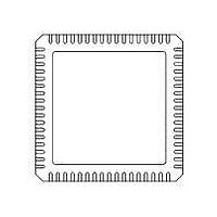
71M6531F-IM/F Maxim Integrated Products, 71M6531F-IM/F Datasheet - Page 12

71M6531F-IM/F
Manufacturer Part Number
71M6531F-IM/F
Description
IC ENERGY METER 256KB 68-QFN
Manufacturer
Maxim Integrated Products
Datasheet
1.71M6531D-IMRF.pdf
(120 pages)
Specifications of 71M6531F-IM/F
Mounting Style
SMD/SMT
Package / Case
QFN-68
Lead Free Status / RoHS Status
Lead free / RoHS Compliant
- Current page: 12 of 120
- Download datasheet (3Mb)
signal sends an FIR_START command to begin the calculation of a sample value from the ADC bit
stream by the FIR. Upon receipt of the FIR_DONE signal from the FIR, the multiplexer will wait until the
next CK32 rising edge to increment its state and initiate the next FIR conversion. FIR conversions require
1, 2, or 3 CK32 cycles. The number of CK32 cycles is determined by FIR_LEN[1:0], as shown in
(see
The purpose of the FIR filter is to decimate the ADC output to the desired resolution. At the end of each
ADC conversion, the output data is stored into the fixed CE RAM location determined by the multiplexer
selection as shown in
voltage output with a predictable temperature coefficient.
The amplifier within the reference is chopper stabilized, i.e. the polarity can be switched by the MPU using
CHOP_E[1:0] (IORAM 0x2002[5:4]). The CHOP_E[1:0] field enables the MPU to operate the chopper circuit
in regular or inverted operation, or in toggling mode. When the chopper circuit is toggled in between
multiplexer cycles, DC offsets on the measured signals will automatically be averaged out.
The general topology of a chopped amplifier is shown in
Data Sheet 71M6531D/F-71M6532D/F
The duration of each multiplexer state depends on the number of ADC samples processed by the FIR,
which is set by FIR_LEN[1:0]. Each multiplexer state will start on the rising edge of CK32. The MUX_CTRL
1.2.3
A single delta-sigma A/D converter digitizes the voltage and current inputs to the 71M6531D/F and
71M6532D/F. The resolution of the ADC is programmable using the I/O RAM M40MHZ and M26MHZ bits
Initiation of each ADC conversion is controlled by MUX_CTRL as described above. At the end of each
ADC conversion, the FIR filter output data is stored into the CE RAM location determined by the MUX
selection.
1.2.4
The finite impulse response filter is an integral part of the ADC and it is optimized for use with the multiplexer.
1.2.5
The device includes an on-chip precision bandgap voltage reference that incorporates auto-zero techniques.
The reference is trimmed to minimize errors caused by component mismatch and drift. The result is a
12
Table
A/D Converter (ADC)
FIR Filter
Voltage References
[M40MHZ, M26MHZ]
2). The CE code must be tailored for use with the selected ADC resolution.
[00], [10] or [11]
Setting for
[01]
Table
Address (HEX)
© 2005-2010 TERIDIAN Semiconductor Corporation
0x00
0x01
0x02
0x03
3. FIR data is stored LSB justified, but shifted left by eight bits.
Table 3: ADC RAM Locations
FIR_LEN[1:0]
Table 2: ADC Resolution
Name
VB
VA
0
1
2
0
1
2
IA
IB
Address (HEX)
Cycles
CK32
Figure
1
2
3
1
2
3
0x0A
0x0B
0x09
3.
FIR CE Cycles
138
288
384
186
384
588
TEMP
Name
VBAT
AUX
FDS 6531/6532 005
Resolution
18 bits
21 bits
22 bits
19 bits
22 bits
24 bits
Table
v1.3
2.
Related parts for 71M6531F-IM/F
Image
Part Number
Description
Manufacturer
Datasheet
Request
R

Part Number:
Description:
IC ENERGY METER 256KB 68-QFN
Manufacturer:
Maxim Integrated Products

Part Number:
Description:
MAX7528KCWPMaxim Integrated Products [CMOS Dual 8-Bit Buffered Multiplying DACs]
Manufacturer:
Maxim Integrated Products
Datasheet:

Part Number:
Description:
Single +5V, fully integrated, 1.25Gbps laser diode driver.
Manufacturer:
Maxim Integrated Products
Datasheet:

Part Number:
Description:
Single +5V, fully integrated, 155Mbps laser diode driver.
Manufacturer:
Maxim Integrated Products
Datasheet:

Part Number:
Description:
VRD11/VRD10, K8 Rev F 2/3/4-Phase PWM Controllers with Integrated Dual MOSFET Drivers
Manufacturer:
Maxim Integrated Products
Datasheet:

Part Number:
Description:
Highly Integrated Level 2 SMBus Battery Chargers
Manufacturer:
Maxim Integrated Products
Datasheet:

Part Number:
Description:
Current Monitor and Accumulator with Integrated Sense Resistor; ; Temperature Range: -40°C to +85°C
Manufacturer:
Maxim Integrated Products

Part Number:
Description:
TSSOP 14/A�/RS-485 Transceivers with Integrated 100O/120O Termination Resis
Manufacturer:
Maxim Integrated Products

Part Number:
Description:
TSSOP 14/A�/RS-485 Transceivers with Integrated 100O/120O Termination Resis
Manufacturer:
Maxim Integrated Products

Part Number:
Description:
QFN 16/A�/AC-DC and DC-DC Peak-Current-Mode Converters with Integrated Step
Manufacturer:
Maxim Integrated Products

Part Number:
Description:
TDFN/A/65V, 1A, 600KHZ, SYNCHRONOUS STEP-DOWN REGULATOR WITH INTEGRATED SWI
Manufacturer:
Maxim Integrated Products

Part Number:
Description:
Integrated Temperature Controller f
Manufacturer:
Maxim Integrated Products

Part Number:
Description:
SOT23-6/I�/45MHz to 650MHz, Integrated IF VCOs with Differential Output
Manufacturer:
Maxim Integrated Products

Part Number:
Description:
SOT23-6/I�/45MHz to 650MHz, Integrated IF VCOs with Differential Output
Manufacturer:
Maxim Integrated Products

Part Number:
Description:
EVALUATION KIT/2.4GHZ TO 2.5GHZ 802.11G/B RF TRANSCEIVER WITH INTEGRATED PA
Manufacturer:
Maxim Integrated Products


