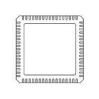
71M6531F-IM/F Maxim Integrated Products, 71M6531F-IM/F Datasheet - Page 45

71M6531F-IM/F
Manufacturer Part Number
71M6531F-IM/F
Description
IC ENERGY METER 256KB 68-QFN
Manufacturer
Maxim Integrated Products
Datasheet
1.71M6531D-IMRF.pdf
(120 pages)
Specifications of 71M6531F-IM/F
Mounting Style
SMD/SMT
Package / Case
QFN-68
Lead Free Status / RoHS Status
Lead free / RoHS Compliant
- Current page: 45 of 120
- Download datasheet (3Mb)
can be configured as dedicated DIO pins, DIO1 and DIO2, respectively (see Section
The internal control resources selectable for the DIO pins are listed in
connected to the same resource, the resources are combined using a logical OR.
With a minimum of 16 driver pins always available and a total of 39 driver pins in the maximum configuration,
the device is capable of driving between 64 to 156 pixels of LCD display with 25% duty cycle. At eight pixels
per digit, this corresponds to 8 to 19 digits. At 33% duty cycle, 48 to 117 pixels can be driven.
For each multi-use pin, the corresponding LCD_BITMAP[] bit (see Section
is used to select the pin for DIO or LCD operation. The mapping of the LCD_BITMAP[] bits is specified in
FDS 6531/6532 005
Additionally, if DIO6 and DIO7 are configured as DIO and defined as outputs, they can be used as
dedicated pulse outputs (WPULSE = DIO6, VARPULSE = DIO7) using the DIO_PW and DIO_PV bits. In
this case, DIO6 and DIO7 are under CE control. DIO4 and DIO5 can be configured to implement the
EEPROM Interface.
The PB pin is a dedicated digital input. In addition, if the optical UART is not used, OPT_TX and OPT_RX
1.5.10 LCD Drivers – 71M6531D/F
The 71M6531 contains a total of 39 dedicated and multiplexed LCD drivers which are grouped as follows:
v1.3
• 11 dedicated LCD segment drivers – always available
• 3 drivers multiplexed with the ICE interface (E_TCLK, E_RST, E_RXTX) – available in normal operation
• 2 driver multiplexed with auxiliary signals MUX_SYNC and CKTEST (SEG7, SEG19) – available
• 4 drivers multiplexed with the SPI port (PCLK, PSDO, PCSZ, PSDI)
• 19 multi-use pins described in Section
• 4 common drivers for multiplexing (25%, 33%, 50%, or 100% duty cycle) – always available
mode (when not emulating)
when not used for test
When driving LEDs, relay coils etc., the DIO pins should sink
Figure 10
tance of the internal switch that connects V3P3D to either V3P3SYS or VBAT.
Tracking DIO pins configured as outputs is useful for pulse counting without external hardware.
Either the interrupts or the counter/timer clocks can be used to count pulses on the pulse outputs
or interrupts on the CE’s power failure output.
Sourcing current into or out of DIO pins other than the PB pin, for example with pull-up or pull-
down resistors, should be avoided. Violating this rule will lead to increased quiescent current in
sleep and LCD modes.
, right), not
HIGH-Z
HIGH
LOW
Figure 10: Connecting an External Load to DIO Pins
© 2005-2010 TERIDIAN Semiconductor Corporation
source it from V3P3D (as shown in
BROWNOUT
MISSION
LCD/SLEEP
DIO
V3P3SYS
V3P3D
GNDD
VBAT
1.5.7 Digital I/O –
71M6531D/F.
Figure 10
HIGH-Z
HIGH
LOW
Data Sheet 71M6531D/F-71M6532D/F
the current into GNDD (as shown in
BROWNOUT
MISSION
LCD/SLEEP
Table
, left). This is due to the resis-
1.5.7 Digital I/O –
46. If more than one input is
DIO
V3P3SYS
VBAT
V3P3D
GNDD
1.5.6 Optical
71M6531D/F),
Interface).
45
Related parts for 71M6531F-IM/F
Image
Part Number
Description
Manufacturer
Datasheet
Request
R

Part Number:
Description:
IC ENERGY METER 256KB 68-QFN
Manufacturer:
Maxim Integrated Products

Part Number:
Description:
MAX7528KCWPMaxim Integrated Products [CMOS Dual 8-Bit Buffered Multiplying DACs]
Manufacturer:
Maxim Integrated Products
Datasheet:

Part Number:
Description:
Single +5V, fully integrated, 1.25Gbps laser diode driver.
Manufacturer:
Maxim Integrated Products
Datasheet:

Part Number:
Description:
Single +5V, fully integrated, 155Mbps laser diode driver.
Manufacturer:
Maxim Integrated Products
Datasheet:

Part Number:
Description:
VRD11/VRD10, K8 Rev F 2/3/4-Phase PWM Controllers with Integrated Dual MOSFET Drivers
Manufacturer:
Maxim Integrated Products
Datasheet:

Part Number:
Description:
Highly Integrated Level 2 SMBus Battery Chargers
Manufacturer:
Maxim Integrated Products
Datasheet:

Part Number:
Description:
Current Monitor and Accumulator with Integrated Sense Resistor; ; Temperature Range: -40°C to +85°C
Manufacturer:
Maxim Integrated Products

Part Number:
Description:
TSSOP 14/A�/RS-485 Transceivers with Integrated 100O/120O Termination Resis
Manufacturer:
Maxim Integrated Products

Part Number:
Description:
TSSOP 14/A�/RS-485 Transceivers with Integrated 100O/120O Termination Resis
Manufacturer:
Maxim Integrated Products

Part Number:
Description:
QFN 16/A�/AC-DC and DC-DC Peak-Current-Mode Converters with Integrated Step
Manufacturer:
Maxim Integrated Products

Part Number:
Description:
TDFN/A/65V, 1A, 600KHZ, SYNCHRONOUS STEP-DOWN REGULATOR WITH INTEGRATED SWI
Manufacturer:
Maxim Integrated Products

Part Number:
Description:
Integrated Temperature Controller f
Manufacturer:
Maxim Integrated Products

Part Number:
Description:
SOT23-6/I�/45MHz to 650MHz, Integrated IF VCOs with Differential Output
Manufacturer:
Maxim Integrated Products

Part Number:
Description:
SOT23-6/I�/45MHz to 650MHz, Integrated IF VCOs with Differential Output
Manufacturer:
Maxim Integrated Products

Part Number:
Description:
EVALUATION KIT/2.4GHZ TO 2.5GHZ 802.11G/B RF TRANSCEIVER WITH INTEGRATED PA
Manufacturer:
Maxim Integrated Products


