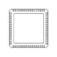
71M6531F-IM/F Maxim Integrated Products, 71M6531F-IM/F Datasheet - Page 90

71M6531F-IM/F
Manufacturer Part Number
71M6531F-IM/F
Description
IC ENERGY METER 256KB 68-QFN
Manufacturer
Maxim Integrated Products
Datasheet
1.71M6531D-IMRF.pdf
(120 pages)
Specifications of 71M6531F-IM/F
Mounting Style
SMD/SMT
Package / Case
QFN-68
Lead Free Status / RoHS Status
Lead free / RoHS Compliant
- Current page: 90 of 120
- Download datasheet (3Mb)
in packed form SAG_CNT, FREQSEL, EXT_PULSE, I0_SHUNT, I1_SHUNT, PULSE_SLOW and PULSE_FAST.
The CECONFIG bit definitions are given in Table 58.
In this case the CE provides an additional gain of 8 to the selected current input. WRATE may need to be
adjusted based on the values of IA_SHUNT and IB_SHUNT. Whenever IA_SHUNT or IB_SHUNT are set to
1, In_8 (in the equation for Kh) is assigned a value of 8.
The CE pulse generator can be controlled by either the MPU (external) or CE (internal) variables. Control
is by the MPU if EXT_PULSE = 1. In this case, the MPU controls the pulse rate by placing values into
APULSEW, APULSER, APULSE2 and APULSE3. By setting EXT_PULSE = 0, the CE controls the pulse rate
based on W0SUM_X and VAR0SUM_X (EQU[2:0] = 0) or WSUM_X (EQU[2:0] = 2).
If EXT_PULSE = 0 and EQU[2:0] = 2, the pulse inputs are W0SUM_X + W1SUM_X and VAR0SUM_X +
VAR1SUM_X. In this case, creep cannot be controlled since creep is an MPU function.
If EXT_PULSE = 0 and EQU[2:0] = 0, the pulse inputs are W0SUM_X if I0SQSUM_X > I1SQSUM_X and
W1SUM_X, if I1SQSUM_X > I0SQSUM_X.
The EXT_TEMP bit controls the temperature compensation mode:
•
•
The FREQSEL1 and FREQSEL0 bits select the phase used to control the CE-internal PLL. CE accuracy
depends on the channel selected by the FREQSEL1 and FREQSEL0 bits receiving a clean voltage signal.
Data Sheet 71M6531D/F-71M6532D/F
The CE is initialized and its functions are controlled by the MPU using CECONFIG. This register contains
IA_SHUNT and/or IB_SHUNT can configure their respective current inputs to accept shunt resistor sensors.
90
CESTATUS [bit]
CE Address
When EXT_TEMP = 0 (internal compensation), the CE will control the gain using GAIN_ADJ (see
based on PPMC, PPMC2 and TEMP_X, the difference between die temperature and the reference /
calibration temperature TEMP_NOM. Since PPMC and PPMC2 reflect the typical behavior of the
reference voltage over temperature, the internal temperature compensation eliminates the effects of
temperature-related errors of VREF only.
When EXT_TEMP = 1 (external compensation), the MPU is allowed to control the CE gain using
GAIN_ADJ, based on any algorithm implemented in MPU code.
0x20
31:29
The 71M6531 Demo Code creep function halts both internal and external pulse generation.
24:0
28
27
26
25
CECONFIG
Reserved
Not Used
Not Used
Name
SAG_B
SAG_A
Name
F0
© 2005-2010 TERIDIAN Semiconductor Corporation
Table 57: CESTATUS (CE RAM 0x80) Bit Definitions
0x5020
These unused bits will always be zero.
F0 is a square wave at the exact fundamental frequency for the
phase selected with the FREQSELn bits in CECONFIG.
Normally zero. Becomes one when VB remains below SAG_THR for
SAG_CNT samples. Will not return to zero until VB rises above
SAG_THR.
Normally zero. Becomes one when VA remains below SAG_THR for
SAG_CNT samples. Will not return to zero until VA rises above
SAG_THR.
These unused bits will always be zero.
Data
See description of the CECONFIG bits in Table 58.
Description
Description
FDS 6531/6532 005
Table
v1.3
60)
Related parts for 71M6531F-IM/F
Image
Part Number
Description
Manufacturer
Datasheet
Request
R

Part Number:
Description:
IC ENERGY METER 256KB 68-QFN
Manufacturer:
Maxim Integrated Products

Part Number:
Description:
MAX7528KCWPMaxim Integrated Products [CMOS Dual 8-Bit Buffered Multiplying DACs]
Manufacturer:
Maxim Integrated Products
Datasheet:

Part Number:
Description:
Single +5V, fully integrated, 1.25Gbps laser diode driver.
Manufacturer:
Maxim Integrated Products
Datasheet:

Part Number:
Description:
Single +5V, fully integrated, 155Mbps laser diode driver.
Manufacturer:
Maxim Integrated Products
Datasheet:

Part Number:
Description:
VRD11/VRD10, K8 Rev F 2/3/4-Phase PWM Controllers with Integrated Dual MOSFET Drivers
Manufacturer:
Maxim Integrated Products
Datasheet:

Part Number:
Description:
Highly Integrated Level 2 SMBus Battery Chargers
Manufacturer:
Maxim Integrated Products
Datasheet:

Part Number:
Description:
Current Monitor and Accumulator with Integrated Sense Resistor; ; Temperature Range: -40°C to +85°C
Manufacturer:
Maxim Integrated Products

Part Number:
Description:
TSSOP 14/A�/RS-485 Transceivers with Integrated 100O/120O Termination Resis
Manufacturer:
Maxim Integrated Products

Part Number:
Description:
TSSOP 14/A�/RS-485 Transceivers with Integrated 100O/120O Termination Resis
Manufacturer:
Maxim Integrated Products

Part Number:
Description:
QFN 16/A�/AC-DC and DC-DC Peak-Current-Mode Converters with Integrated Step
Manufacturer:
Maxim Integrated Products

Part Number:
Description:
TDFN/A/65V, 1A, 600KHZ, SYNCHRONOUS STEP-DOWN REGULATOR WITH INTEGRATED SWI
Manufacturer:
Maxim Integrated Products

Part Number:
Description:
Integrated Temperature Controller f
Manufacturer:
Maxim Integrated Products

Part Number:
Description:
SOT23-6/I�/45MHz to 650MHz, Integrated IF VCOs with Differential Output
Manufacturer:
Maxim Integrated Products

Part Number:
Description:
SOT23-6/I�/45MHz to 650MHz, Integrated IF VCOs with Differential Output
Manufacturer:
Maxim Integrated Products

Part Number:
Description:
EVALUATION KIT/2.4GHZ TO 2.5GHZ 802.11G/B RF TRANSCEIVER WITH INTEGRATED PA
Manufacturer:
Maxim Integrated Products


