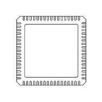
71M6531F-IM/F Maxim Integrated Products, 71M6531F-IM/F Datasheet - Page 77

71M6531F-IM/F
Manufacturer Part Number
71M6531F-IM/F
Description
IC ENERGY METER 256KB 68-QFN
Manufacturer
Maxim Integrated Products
Datasheet
1.71M6531D-IMRF.pdf
(120 pages)
Specifications of 71M6531F-IM/F
Mounting Style
SMD/SMT
Package / Case
QFN-68
Lead Free Status / RoHS Status
Lead free / RoHS Compliant
- Current page: 77 of 120
- Download datasheet (3Mb)
FDS 6531/6532 005
4.2
The following conventions apply to the descriptions in this table:
•
•
•
•
v1.3
ADC_E
BME
BOOT_SIZE[7:0] 20A7[7:0]
CE10MHZ
CE_E
CE_LCTN[7:0]
CHOP_E[1:0]
CHOP_IA
CHOP_IB
CHOP_I_E
CKOUT_E
Bits with a W (write) direction are written by the MPU into configuration RAM. Typically, they are initially stored in flash memory and copied to
the configuration RAM by the MPU. Some of the more frequently programmed bits are mapped to the MPU SFR memory space. The remaining
bits are mapped to 2xxx.
Bits with a R (read) direction can be read by the MPU.
Columns labeled Reset and Wake describe the bit values upon reset and wake, respectively. “NV” in the Wake column means the bit is powered
by the nonvolatile supply and is not initialized. LCD-related registers labeled “L” retain data upon transition from LCD mode to BROWNOUT
mode and vice versa, but do not retain data in SLEEP mode. “–“ means that the value is undefined.
Write-only bits will return zero when they are read.
Name
I/O RAM Description – Alphabetical Order
2005[3]
2020[6]
2000[3]
2000[4]
20A8[4:0]
2002[5:4]
20AC[0]
20AC[4]
20AB[0]
2004[4]
Location
Reset
01
31
0
0
0
0
0
0
0
0
0
Wake
01
31
0
–
0
0
0
0
0
0
0
© 2005-2010 TERIDIAN Semiconductor Corporation
Table 55: I/O RAM Description - Alphabetical
R/W
R/W
R/W
R/W
R/W
R/W
R/W
R/W
R/W
R/W
R/W
Dir
must be set also.
Enables ADC and VREF. When disabled, removes bias current.
Battery Measure Enable. When set, a load current is immediately applied to the battery
and it is connected to the ADC to be measured on Alternative Mux Cycles. See the
MUX_ALT bit.
End of space reserved for boot program. The ending address of the boot region is
1024*BOOT_SIZE.
CE clock select. When set, the CE is clocked at 10 MHz. Otherwise, the CE clock
frequency is 5 MHz.
CE enable.
CE program location. The starting address for the CE program is 1024*CE_LCTN.
Chop enable for the reference bandgap circuit. The value of CHOP will change on the
rising edge of MUXSYNC according to the value in CHOP_E[1:0]:
This bit enables chop mode for the IA current channel (71M6532D/F only). CHOP_I_E
must be set also.
This bit enables chop mode for the IB current channel (71M6532D/F only). CHOP_I_E
This bit must be set to enable chop mode for the current channels (71M6532D/F only).
Control bit for the SEG19/CKOUT pin:
0: The pin is the SEG19 LCD driver
1: The pin is the CK_FIR output (5 MHz in mission mode, 32 kHz in brownout mode)
00 = toggle, except at the mux sync edge at the end of SUMCYCLE, an alternative
MUX frame is automatically inserted at the end of each accumulation interval.
01 = positive.
10 = reversed.
11 = toggle, no alternative MUX frame is inserted
Description
Data Sheet 71M6531D/F-71M6532D/F
77
Related parts for 71M6531F-IM/F
Image
Part Number
Description
Manufacturer
Datasheet
Request
R

Part Number:
Description:
IC ENERGY METER 256KB 68-QFN
Manufacturer:
Maxim Integrated Products

Part Number:
Description:
MAX7528KCWPMaxim Integrated Products [CMOS Dual 8-Bit Buffered Multiplying DACs]
Manufacturer:
Maxim Integrated Products
Datasheet:

Part Number:
Description:
Single +5V, fully integrated, 1.25Gbps laser diode driver.
Manufacturer:
Maxim Integrated Products
Datasheet:

Part Number:
Description:
Single +5V, fully integrated, 155Mbps laser diode driver.
Manufacturer:
Maxim Integrated Products
Datasheet:

Part Number:
Description:
VRD11/VRD10, K8 Rev F 2/3/4-Phase PWM Controllers with Integrated Dual MOSFET Drivers
Manufacturer:
Maxim Integrated Products
Datasheet:

Part Number:
Description:
Highly Integrated Level 2 SMBus Battery Chargers
Manufacturer:
Maxim Integrated Products
Datasheet:

Part Number:
Description:
Current Monitor and Accumulator with Integrated Sense Resistor; ; Temperature Range: -40°C to +85°C
Manufacturer:
Maxim Integrated Products

Part Number:
Description:
TSSOP 14/A�/RS-485 Transceivers with Integrated 100O/120O Termination Resis
Manufacturer:
Maxim Integrated Products

Part Number:
Description:
TSSOP 14/A�/RS-485 Transceivers with Integrated 100O/120O Termination Resis
Manufacturer:
Maxim Integrated Products

Part Number:
Description:
QFN 16/A�/AC-DC and DC-DC Peak-Current-Mode Converters with Integrated Step
Manufacturer:
Maxim Integrated Products

Part Number:
Description:
TDFN/A/65V, 1A, 600KHZ, SYNCHRONOUS STEP-DOWN REGULATOR WITH INTEGRATED SWI
Manufacturer:
Maxim Integrated Products

Part Number:
Description:
Integrated Temperature Controller f
Manufacturer:
Maxim Integrated Products

Part Number:
Description:
SOT23-6/I�/45MHz to 650MHz, Integrated IF VCOs with Differential Output
Manufacturer:
Maxim Integrated Products

Part Number:
Description:
SOT23-6/I�/45MHz to 650MHz, Integrated IF VCOs with Differential Output
Manufacturer:
Maxim Integrated Products

Part Number:
Description:
EVALUATION KIT/2.4GHZ TO 2.5GHZ 802.11G/B RF TRANSCEIVER WITH INTEGRATED PA
Manufacturer:
Maxim Integrated Products


