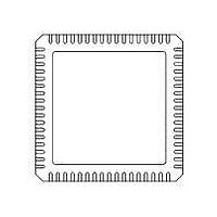
71M6531F-IM/F Maxim Integrated Products, 71M6531F-IM/F Datasheet - Page 40

71M6531F-IM/F
Manufacturer Part Number
71M6531F-IM/F
Description
IC ENERGY METER 256KB 68-QFN
Manufacturer
Maxim Integrated Products
Datasheet
1.71M6531D-IMRF.pdf
(120 pages)
Specifications of 71M6531F-IM/F
Mounting Style
SMD/SMT
Package / Case
QFN-68
Lead Free Status / RoHS Status
Lead free / RoHS Compliant
the primary boot sequence begins). Once security is enabled, the only way to disable it is to perform a
global erase of the flash, followed by a chip reset.
but may not reset it. Once SECURE is set, the pre-boot code is protected and no external read of program
code is possible
Specifically, when SECURE is set, the following applies:
•
•
•
MPU/CE RAM:
The 71M6531D/F and 71M6532D/F include 4 KB of static RAM memory on-chip (XRAM) plus 256-bytes
of internal RAM in the MPU core. The 4 KB of static RAM are used for data storage for MPU and CE
operations.
system power is present (i.e. not in BROWNOUT mode). The OPT_TXMOD bit enables modulation. Duty
cycle is controlled by OPT_FDC[1:0], which can select 50%, 25%, 12.5% and 6.25% duty cycle. 6.25% duty
cycle means OPT_TX is low for 6.25% of the period.
When not needed for the optical UART, the OPT_TX pin can alternatively be configured as DIO2,
WPULSE, or VARPULSE. The configuration bits are OPT_TXE[1:0]. Likewise, OPT_RX can alternately
be configured as DIO1. Its control is OPT_RXDIS.
Data Sheet 71M6531D/F-71M6532D/F
Program Security
When enabled, the security feature limits the ICE to global flash erase operations only. All other ICE
operations are blocked. This guarantees the security of the user’s MPU and CE program code. Security
should be enabled by MPU code that is executed during the pre-boot interval (60 CKMPU cycles before
The first 60 cycles of the MPU boot code are called the pre-boot phase because during this phase the
ICE is inhibited. A read-only status bit, PREBOOT, identifies these cycles to the MPU. Upon completion
of pre-boot, the ICE can be enabled and is permitted to take control of the MPU.
The security enable bit, SECURE, is reset whenever the chip is reset. Hardware associated with the bit
permits only ones to be written to it. Thus, pre-boot code may set SECURE to enable the security feature
1.5.6
The device includes an interface to implement an IR/optical port. The pin OPT_TX is designed to directly
drive an external LED for transmitting data on an optical link. The pin OPT_RX has the same threshold
as the RX pin, but can also be used to sense the input from an external photo detector used as the receiver
for the optical link. OPT_TX and OPT_RX are connected to a dedicated UART port (UART1).
The OPT_TX and OPT_RX pins can be inverted with configuration bits OPT_TXINV and OPT_RXINV,
respectively. Additionally, the OPT_TX output may be modulated at 38 kHz. Modulation is available when
40
The ICE is limited to bulk flash erase only.
Page zero of flash memory, the preferred location for the user’s pre-boot code, may not be
page-erased by either MPU or ICE. Page zero may only be erased with global flash erase.
Write operations to page zero, whether by MPU or ICE are inhibited.
FL_BANK [1:0]
Optical Interface
71M6531D
000
001
010
011
FL_BANK [2:0]
© 2005-2010 TERIDIAN Semiconductor Corporation
71M653XF
Table 38: Bank Switching with FL_BANK[2:0]
000
001
010
011
100
101
110
111
Address Range for Lower
Bank (0x000-0x7FFF)
0x0000-0x7FFF
Figure 9
illustrates the OPT_TX generator.
Address Range for Upper
Bank (0x8000-0xFFFF)
0x18000-0x1FFFF
0x28000-0x2FFFF
0x38000-0x3FFFF
0x10000-0x17FFF
0x20000-0x217FF
0x30000-0x37FFF
0x8000-0xFFFF
0x0000-0x7FFF
FDS 6531/6532 005
v1.3


