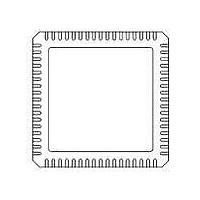
71M6531F-IM/F Maxim Integrated Products, 71M6531F-IM/F Datasheet - Page 24

71M6531F-IM/F
Manufacturer Part Number
71M6531F-IM/F
Description
IC ENERGY METER 256KB 68-QFN
Manufacturer
Maxim Integrated Products
Datasheet
1.71M6531D-IMRF.pdf
(120 pages)
Specifications of 71M6531F-IM/F
Mounting Style
SMD/SMT
Package / Case
QFN-68
Lead Free Status / RoHS Status
Lead free / RoHS Compliant
- Current page: 24 of 120
- Download datasheet (3Mb)
driver and an input buffer, therefore the MPU can output or read data through any of these ports. Even if
a DIO pin is configured as an output, the state of the pin can still be read by the MPU, for example when
counting pulses issued via DIO pins that are under CE control.
Clock Stretching (CKCON[2:0], SFR 0x8E)
The CKCON[2:0] field defines the stretch memory cycles that could be used for MOVX instructions when
accessing slow external peripherals. The practical value of this register for the 71M653x is to guarantee
access to XRAM between CE, MPU, and SPI. The default setting of CKCON[2:0] (001) should not be
changed.Table 13 shows how the signals of the External Memory Interface change when stretch values
are set from 0 to 7. The widths of the signals are counted in MPU clock cycles. The post-reset state of
the CKCON[2:0] field (001), which is shown in bold in the table, performs the MOVX instructions with a
stretch value equal to 1.
Data Sheet 71M6531D/F-71M6532D/F
All DIO ports on the chip are bi-directional. Each of them consists of a Latch (SFR P0 to P2), an output
1.4.4
Table 14
24
EEDATA
EECTRL
P0
DIR0
P1
DIR1
P2
DIR2
Register
(Alternate Name)
Register
outputs can be used to implement pulse counting.
The technique of reading the status of or generating interrupts based on DIO pins configured as
Special Function Registers (SFRs) Specific to the 71M6531D/F and 71M6532D/F
shows the location and description of the SFRs specific to the 71M6531D/F and 71M6532D/F.
Address
CKCON[2:0]
0xA2
0xA0
0xA1
0x80
0x90
0x91
SFR
000
001
010
011
100
101
110
111
Table 14: 71M6531D/F and 71M6532D/F Specific SFRs
Address
R/W
R/W
R/W
R/W
R/W
R/W
R/W
© 2005-2010 TERIDIAN Semiconductor Corporation
0x9E
0x9F
SFR
Register for port 0 read and write operations.
Data direction register for port 0. Setting a bit to 1 indicates that the
corresponding pin is an output.
Register for port 1 read and write operations.
Data direction register for port 1.
Register for port 2 read and write operations.
Data direction register for port 2.
Stretch
Table 13: Stretch Memory Cycle Width
Value
0
1
2
3
4
5
6
7
Bit Field
Name
Table 12: Port Registers
memaddr
Read signal width
1
2
3
4
5
6
7
8
R/W
R/W I
R/W
memrd
I
Section
description of the command and status bits
available for EECTRL.
2
2
C EEPROM interface data register.
C EEPROM interface control register. See
1
2
3
4
5
6
7
8
Description
1.5.14 EEPROM Interface
memaddr
Write signal width
2
3
4
5
6
7
8
9
Description
memwr
FDS 6531/6532 005
1
1
2
3
4
5
6
7
for a
v1.3
Related parts for 71M6531F-IM/F
Image
Part Number
Description
Manufacturer
Datasheet
Request
R

Part Number:
Description:
IC ENERGY METER 256KB 68-QFN
Manufacturer:
Maxim Integrated Products

Part Number:
Description:
MAX7528KCWPMaxim Integrated Products [CMOS Dual 8-Bit Buffered Multiplying DACs]
Manufacturer:
Maxim Integrated Products
Datasheet:

Part Number:
Description:
Single +5V, fully integrated, 1.25Gbps laser diode driver.
Manufacturer:
Maxim Integrated Products
Datasheet:

Part Number:
Description:
Single +5V, fully integrated, 155Mbps laser diode driver.
Manufacturer:
Maxim Integrated Products
Datasheet:

Part Number:
Description:
VRD11/VRD10, K8 Rev F 2/3/4-Phase PWM Controllers with Integrated Dual MOSFET Drivers
Manufacturer:
Maxim Integrated Products
Datasheet:

Part Number:
Description:
Highly Integrated Level 2 SMBus Battery Chargers
Manufacturer:
Maxim Integrated Products
Datasheet:

Part Number:
Description:
Current Monitor and Accumulator with Integrated Sense Resistor; ; Temperature Range: -40°C to +85°C
Manufacturer:
Maxim Integrated Products

Part Number:
Description:
TSSOP 14/A�/RS-485 Transceivers with Integrated 100O/120O Termination Resis
Manufacturer:
Maxim Integrated Products

Part Number:
Description:
TSSOP 14/A�/RS-485 Transceivers with Integrated 100O/120O Termination Resis
Manufacturer:
Maxim Integrated Products

Part Number:
Description:
QFN 16/A�/AC-DC and DC-DC Peak-Current-Mode Converters with Integrated Step
Manufacturer:
Maxim Integrated Products

Part Number:
Description:
TDFN/A/65V, 1A, 600KHZ, SYNCHRONOUS STEP-DOWN REGULATOR WITH INTEGRATED SWI
Manufacturer:
Maxim Integrated Products

Part Number:
Description:
Integrated Temperature Controller f
Manufacturer:
Maxim Integrated Products

Part Number:
Description:
SOT23-6/I�/45MHz to 650MHz, Integrated IF VCOs with Differential Output
Manufacturer:
Maxim Integrated Products

Part Number:
Description:
SOT23-6/I�/45MHz to 650MHz, Integrated IF VCOs with Differential Output
Manufacturer:
Maxim Integrated Products

Part Number:
Description:
EVALUATION KIT/2.4GHZ TO 2.5GHZ 802.11G/B RF TRANSCEIVER WITH INTEGRATED PA
Manufacturer:
Maxim Integrated Products


