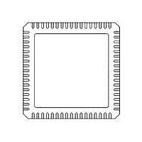
71M6531F-IM/F Maxim Integrated Products, 71M6531F-IM/F Datasheet - Page 19

71M6531F-IM/F
Manufacturer Part Number
71M6531F-IM/F
Description
IC ENERGY METER 256KB 68-QFN
Manufacturer
Maxim Integrated Products
Datasheet
1.71M6531D-IMRF.pdf
(120 pages)
Specifications of 71M6531F-IM/F
Mounting Style
SMD/SMT
Package / Case
QFN-68
Lead Free Status / RoHS Status
Lead free / RoHS Compliant
instructions in one clock cycle. Using a 10-MHz clock results in a processing throughput of 10 MIPS. The
80515 architecture eliminates redundant bus states and implements parallel execution of fetch and execution
phases. Normally, a machine cycle is aligned with a memory fetch, therefore, most of the 1-byte instructions
are performed in a single machine cycle (MPU clock cycle). This leads to an 8x average performance
improvement (in terms of MIPS) over the Intel
Table 6
MPU_DIV[2:0] and the MCK divider bits M40MHZ and M26MHZ. Actual processor clocking speed can be
adjusted to the total processing demand of the application (metering calculations, AMR management, memo-
ry management, LCD driver management and I/O management) using the I/O RAM field MPU_DIV[2:0]
and the MCK divider bits M40MHZ and M26MHZ, as shown in
source code to help reduce the design cycle.
Program Memory
The 80515 can address up to 64 KB of program memory space from 0x0000 to 0xFFFF. Program memory
is read when the MPU fetches instructions or performs a MOVC operation. Access to program memory
above 0x7FFF is controlled by the FL_BANK[2:0] register (SFR 0xB6).
After reset, the MPU starts program execution from program memory location 0x0000. The lower part of
the program memory includes reset and interrupt vectors. The interrupt vectors are spaced at 8-byte
intervals, starting from 0x0003.
MPU External Data Memory (XRAM)
Both internal and external memory is physically located on the 71M6531 device. The external memory
referred to in this documentation is only external to the 80515 MPU core.
4 KB of RAM starting at address 0x0000 is shared by the CE and MPU. The CE normally uses the first
1 KB, leaving 3 KB for the MPU. Different versions of the CE code use varying amounts. Consult the
documentation for the specific code version being used for the exact limit.
FDS 6531/6532 005
1.4
The 71M6531D/F and 71M6532D/F include an 80515 MPU (8-bit, 8051-compatible) that processes most
Typical measurement and metering functions based on the results provided by the internal 32-bit compute
engine (CE) are available for the MPU as part of Teridian’s standard library. Teridian provides demonstration
1.4.1
The 80515 MPU core incorporates the Harvard architecture with separate code and data spaces. Memory
organization in the 80515 is similar to that of the industry standard 8051. There are four memory areas:
Program memory (Flash, shared by MPU and CE), external RAM (Data RAM, shared by the CE and MPU,
Configuration or I/O RAM), and internal data memory (Internal RAM).
v1.3
If the MPU overwrites the CE’s working RAM, the CE’s output may be corrupted. If the CE is disabled,
the first 0x40 bytes of RAM are still unusable while MUX_DIV[3:0] ≠ 0 because the 71M6531 ADC
writes to these locations. Setting MUX_DIV[3:0] = 0 disables the ADC output preventing the CE from
writing the first 0x40 bytes of RAM.
80515 MPU Core
shows the CKMPU frequency as a function of the allowed combinations of the MPU clock divider
Memory Organization and Addressing
MPU_DIV [2:0]
© 2005-2010 TERIDIAN Semiconductor Corporation
000
001
010
011
100
101
110
111
Table 6: CKMPU Clock Frequencies
9.8304 MHz
4.9152 MHz
2.4576 MHz
1.2288 MHz
614.4 kHz
307.2 kHz
153.6 kHz
153.6 kHz
[1,0]
8051 device running at the same clock frequency.
[M40MHZ, M26MHZ] Values
6.5536 MHz
3.2768 MHz
1.6384 MHz
819.2 kHz
409.6 kHz
204.8 kHz
102.4 kHz
102.4 kHz
[0,1]
Table
Data Sheet 71M6531D/F-71M6532D/F
6.
Table 7
4.9152 MHz
2.4576 MHz
1.2288 MHz
614.4 kHz
307.2 kHz
153.6 kHz
76.80 kHz
76.8 kHz
[0,0]
shows the memory map.
19


