C8051F226DK Silicon Laboratories Inc, C8051F226DK Datasheet - Page 101
C8051F226DK
Manufacturer Part Number
C8051F226DK
Description
DEV KIT F220/221/226/230/231/236
Manufacturer
Silicon Laboratories Inc
Type
MCUr
Datasheet
1.C8051F226DK.pdf
(146 pages)
Specifications of C8051F226DK
Contents
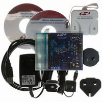
Evaluation Board, Power Supply, USB Cables, Adapter and Documentation
Processor To Be Evaluated
C8051F22x and C8051F23x
Interface Type
USB
Silicon Manufacturer
Silicon Labs
Core Architecture
8051
Silicon Core Number
C8051F226
Silicon Family Name
C8051F2xx
Lead Free Status / RoHS Status
Contains lead / RoHS non-compliant
For Use With/related Products
C8051F220, 221, 226, 230, 231, 236
Lead Free Status / Rohs Status
Lead free / RoHS Compliant
Other names
336-1241


14. Port Input/Output
Description
The C8051F221/231 have three I/O Ports: Port0, Port1, and Port2. The C8051F206, C8051F220/6 and
C8051F230/6 have four I/O Ports: Port0, Port1, Port2, and Port3. A wide array of digital resources can be
assigned to these ports by the simple configuration of the port's corresponding multiplexer (MUX). Please
see Figure 8.1. Additionally, all external port pins are available as analog input.
14.1. Port I/O Initialization
Port I/O initialization is straightforward. Registers PRT0MX, PRT1MX and PRT2MX must be loaded with
the appropriate values to select the digital I/O functions required by the design. The output driver charac-
teristics of the I/O pins are defined using the Port Configuration Registers PRT0CF, PRT1CF, PRT2CF and
PRT3CF. Each Port Output driver can be configured as either Open Drain or Push-Pull. This is required
even for the digital resources selected in the PRTnMX registers, and is not automatic.
Any or all pins may be configured as digital I/O or as analog input. The default mode is digital I/O. The
P0MODE, P1MODE, P2MODE, and P3MODE special function registers are used to configure the port
pins as digital or analog as defined in this section.
The final step is initializing the individual resources selected using the appropriate setup registers. Initial-
ization procedures for the various digital resources may be found in the detailed explanation of each avail-
able function. The reset state of each register is shown in the figures that describe each individual register.
1. The output mode of all ports pins must be configured regardless of whether the port pin is
2. For all pins used as Timer inputs (P0.4/T0, P0.5/T1, P0.6/T2, and P0.7/T2EX), the output
figured.
NOTE: The input mode of pins configured for use with Timer 0, 1, or 2 must be manually con-
either standard general-purpose I/O or controlled by a digital peripheral.
mode must be "open-drain" (which is the reset state), and "1" must be written to the associated
port pin to prevent possible contention for the port pin that could result in an overcurrent condi-
tion. For example, to configure a Timer0, set PRT0MX's T0E Timer0 enable bit to '1' to route
Timer0 to Port Pin P0.4. Then place P0.4/T0 in open-drain configuration (which is set in
PRT0CF by default), and write a '1' to P0.4 to set its output state to high impedance for use as
a digital peripheral input (port pins also default to logic high state upon reset). Lastly, ensure
P0MODE.4 is '1' for digital input mode. (All pins default to digital input mode upon reset.)
Rev. 1.6
C8051F2xx
101
Related parts for C8051F226DK
Image
Part Number
Description
Manufacturer
Datasheet
Request
R

Part Number:
Description:
SMD/C°/SINGLE-ENDED OUTPUT SILICON OSCILLATOR
Manufacturer:
Silicon Laboratories Inc
Part Number:
Description:
Manufacturer:
Silicon Laboratories Inc
Datasheet:
Part Number:
Description:
N/A N/A/SI4010 AES KEYFOB DEMO WITH LCD RX
Manufacturer:
Silicon Laboratories Inc
Datasheet:
Part Number:
Description:
N/A N/A/SI4010 SIMPLIFIED KEY FOB DEMO WITH LED RX
Manufacturer:
Silicon Laboratories Inc
Datasheet:
Part Number:
Description:
N/A/-40 TO 85 OC/EZLINK MODULE; F930/4432 HIGH BAND (REV E/B1)
Manufacturer:
Silicon Laboratories Inc
Part Number:
Description:
EZLink Module; F930/4432 Low Band (rev e/B1)
Manufacturer:
Silicon Laboratories Inc
Part Number:
Description:
I°/4460 10 DBM RADIO TEST CARD 434 MHZ
Manufacturer:
Silicon Laboratories Inc
Part Number:
Description:
I°/4461 14 DBM RADIO TEST CARD 868 MHZ
Manufacturer:
Silicon Laboratories Inc
Part Number:
Description:
I°/4463 20 DBM RFSWITCH RADIO TEST CARD 460 MHZ
Manufacturer:
Silicon Laboratories Inc
Part Number:
Description:
I°/4463 20 DBM RADIO TEST CARD 868 MHZ
Manufacturer:
Silicon Laboratories Inc
Part Number:
Description:
I°/4463 27 DBM RADIO TEST CARD 868 MHZ
Manufacturer:
Silicon Laboratories Inc
Part Number:
Description:
I°/4463 SKYWORKS 30 DBM RADIO TEST CARD 915 MHZ
Manufacturer:
Silicon Laboratories Inc
Part Number:
Description:
N/A N/A/-40 TO 85 OC/4463 RFMD 30 DBM RADIO TEST CARD 915 MHZ
Manufacturer:
Silicon Laboratories Inc
Part Number:
Description:
I°/4463 20 DBM RADIO TEST CARD 169 MHZ
Manufacturer:
Silicon Laboratories Inc