C8051F226DK Silicon Laboratories Inc, C8051F226DK Datasheet - Page 87
C8051F226DK
Manufacturer Part Number
C8051F226DK
Description
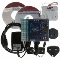
DEV KIT F220/221/226/230/231/236
Manufacturer
Silicon Laboratories Inc
Type
MCUr
Datasheet
1.C8051F226DK.pdf
(146 pages)
Specifications of C8051F226DK
Contents
Evaluation Board, Power Supply, USB Cables, Adapter and Documentation
Processor To Be Evaluated
C8051F22x and C8051F23x
Interface Type
USB
Silicon Manufacturer
Silicon Labs
Core Architecture
8051
Silicon Core Number
C8051F226
Silicon Family Name
C8051F2xx
Lead Free Status / RoHS Status
Contains lead / RoHS non-compliant
For Use With/related Products
C8051F220, 221, 226, 230, 231, 236
Lead Free Status / Rohs Status
Lead free / RoHS Compliant
Other names
336-1241


The lock bits can always be read and cleared to logic 0 regardless of the security setting applied to the
block containing the security bytes. This allows additional blocks to be protected after the block containing
the security bytes has been locked. However, the only means of removing a lock once set is to erase the
entire program memory space by performing a JTAG erase operation. NOTE: Erasing the Flash memory
block containing the security bytes will automatically initiate erasure of the entire program memory space
(except for the reserved area). This erasure can only be performed via the JTAG. If a non-security byte in
the 0x1C00–0x1DFF page is written to in order to perform an erasure of that page, then that page including
the security bytes will be erased.
Flash Read Lock Byte
Bits7–0: Each bit locks a corresponding block of memory. (Bit 7 is MSB.)
Flash Write/Erase Lock Byte
Flash Access Limit Register (FLACL)
Program Memory
Bits7–0: Each bit locks a corresponding block of memory.
Space
0: Read operations are locked (disabled) for corresponding block across the JTAG inter-
face.
1: Read operations are unlocked (enabled) for corresponding block across the JTAG inter-
face.
0: Write/Erase operations are locked (disabled) for corresponding block across the JTAG
interface.
1: Write/Erase operations are unlocked (enabled) for corresponding block across the
JTAG interface.
The content of this register is used as the high byte of the 16-bit software read limit
address. The 16-bit read limit address value is calculated as 0xNN00 where NN is
replaced by content of this register on reset. Software running at or above this address is
prohibited from using the MOVX and MOVC instructions to read, write, or erase, locations
below this address. Any attempts to read locations below this limit will return the value
0x00.
Figure 10.1. Flash Program Memory Security Bytes
(This Block locked only if all
Write/Erase Lock Byte
other blocks are locked)
Software Read Limit
Read Lock Byte
Reserved
Rev. 1.6
0x207F
0x2000
0x1FFF
0x1E00
0x1DFF
0x1DF
E
0x1DFD
0x0000
Read and Write/Erase Security Bits.
(Bit 7 is MSB.)
Bit
7
6
5
4
3
2
1
0
0x1C00 - 0x1DFD
0x0C00 - 0x0FFF
0x1800 - 0x1BFF
0x0800 - 0x0BFF
Memory Block
0x1400 - 0x17FF
0x1000 - 0x13FF
0x0400 - 0x07FF
0x0000 - 0x03FF
C8051F2xx
87
Related parts for C8051F226DK
Image
Part Number
Description
Manufacturer
Datasheet
Request
R

Part Number:
Description:
SMD/C°/SINGLE-ENDED OUTPUT SILICON OSCILLATOR
Manufacturer:
Silicon Laboratories Inc
Part Number:
Description:
Manufacturer:
Silicon Laboratories Inc
Datasheet:
Part Number:
Description:
N/A N/A/SI4010 AES KEYFOB DEMO WITH LCD RX
Manufacturer:
Silicon Laboratories Inc
Datasheet:
Part Number:
Description:
N/A N/A/SI4010 SIMPLIFIED KEY FOB DEMO WITH LED RX
Manufacturer:
Silicon Laboratories Inc
Datasheet:
Part Number:
Description:
N/A/-40 TO 85 OC/EZLINK MODULE; F930/4432 HIGH BAND (REV E/B1)
Manufacturer:
Silicon Laboratories Inc
Part Number:
Description:
EZLink Module; F930/4432 Low Band (rev e/B1)
Manufacturer:
Silicon Laboratories Inc
Part Number:
Description:
I°/4460 10 DBM RADIO TEST CARD 434 MHZ
Manufacturer:
Silicon Laboratories Inc
Part Number:
Description:
I°/4461 14 DBM RADIO TEST CARD 868 MHZ
Manufacturer:
Silicon Laboratories Inc
Part Number:
Description:
I°/4463 20 DBM RFSWITCH RADIO TEST CARD 460 MHZ
Manufacturer:
Silicon Laboratories Inc
Part Number:
Description:
I°/4463 20 DBM RADIO TEST CARD 868 MHZ
Manufacturer:
Silicon Laboratories Inc
Part Number:
Description:
I°/4463 27 DBM RADIO TEST CARD 868 MHZ
Manufacturer:
Silicon Laboratories Inc
Part Number:
Description:
I°/4463 SKYWORKS 30 DBM RADIO TEST CARD 915 MHZ
Manufacturer:
Silicon Laboratories Inc
Part Number:
Description:
N/A N/A/-40 TO 85 OC/4463 RFMD 30 DBM RADIO TEST CARD 915 MHZ
Manufacturer:
Silicon Laboratories Inc
Part Number:
Description:
I°/4463 20 DBM RADIO TEST CARD 169 MHZ
Manufacturer:
Silicon Laboratories Inc