C8051F226DK Silicon Laboratories Inc, C8051F226DK Datasheet - Page 119
C8051F226DK
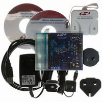
Manufacturer Part Number
C8051F226DK
Description
DEV KIT F220/221/226/230/231/236
Manufacturer
Silicon Laboratories Inc
Type
MCUr
Datasheet
1.C8051F226DK.pdf
(146 pages)
Specifications of C8051F226DK
Contents
Evaluation Board, Power Supply, USB Cables, Adapter and Documentation
Processor To Be Evaluated
C8051F22x and C8051F23x
Interface Type
USB
Silicon Manufacturer
Silicon Labs
Core Architecture
8051
Silicon Core Number
C8051F226
Silicon Family Name
C8051F2xx
Lead Free Status / RoHS Status
Contains lead / RoHS non-compliant
For Use With/related Products
C8051F220, 221, 226, 230, 231, 236
Lead Free Status / Rohs Status
Lead free / RoHS Compliant
Other names
336-1241


16.1.2. Mode 1: 8-Bit UART, Variable Baud Rate
Mode 1 provides standard asynchronous, full duplex communication using a total of 10 bits per data byte:
one start bit, eight data bits (LSB first), and one stop bit (see the timing diagram in Figure 16.4). Data are
transmitted from the TX pin and received at the RX pin (see the interconnection diagram in Figure 16.5).
On receive, the eight data bits are stored in SBUF and the stop bit goes into RB8 (SCON.2).
Data transmission begins when an instruction writes a data byte to the SBUF register. The TI Transmit
Interrupt Flag (SCON.1) is set at the end of the transmission (the beginning of the stop-bit time). Data
reception can begin any time after the REN Receive Enable bit (SCON.4) is set to logic 1. After the stop bit
is received, the data byte will be loaded into the SBUF receive register if the following conditions are met:
RI must be logic 0, and if SM2 is logic 1, the stop bit must be logic 1.
If these conditions are met, the eight bits of data are stored in SBUF, the stop bit is stored in RB8, and the
RI flag is set. If these conditions are not met, SBUF and RB8 will not be loaded and the RI flag will not be
set. An interrupt will occur if enabled when either TI or RI is set.
The baud rate generated in Mode 1 is a function of timer overflow. The UART can use Timer 1 operating in
8-bit Counter/Timer with Auto-Reload Mode, or Timer 2 operating in Baud Rate Generator Mode to gener-
ate the baud rate (note that the TX and RX clock sources are selected separately). On each timer overflow
event (a rollover from all ones (0xFF for Timer 1, 0xFFFF for Timer 2) to zero), a clock is sent to the baud
rate logic.
When Timer 1 is selected as a baud rate source, the SMOD bit (PCON.7) selects whether or not to divide
the Timer 1 overflow rate by two. On reset, the SMOD bit is logic 0, thus selecting the lower speed baud
rate by default. The SMOD bit affects the baud rate generated by Timer 1 as follows:
When Timer 2 is selected as a baud rate source, the baud rate generated by Timer 2 is as follows:
The Timer 1 overflow rate is determined by the Timer 1 clock source (T1CLK) and reload value (TH1). The
frequency of T1CLK can be selected as SYSCLK, SYSCLK/12, or an external clock source. The Timer 1
overflow rate can be calculated as follows:
For example, assume TMOD = 0x20.
SPACE
Mode 1 Baud Rate = (1 / 32) x T1_OVERFLOWRATE (when the SMOD bit is set to logic 0).
Mode 1 Baud Rate = (1 / 16) x T1_OVERFLOWRATE (when the SMOD bit is set to logic 1).
MARK
BIT TIMES
BIT SAMPLING
START
BIT
Figure 16.4. UART Mode 1 Timing Diagram
Mode 1 Baud Rate = (1 / 16) x T2_OVERFLOWRATE.
D0
T1_OVERFLOWRATE = T1CLK / (256 – TH1).
D1
D2
Rev. 1.6
D3
D4
D5
D6
C8051F2xx
D7
STOP
BIT
119
Related parts for C8051F226DK
Image
Part Number
Description
Manufacturer
Datasheet
Request
R

Part Number:
Description:
SMD/C°/SINGLE-ENDED OUTPUT SILICON OSCILLATOR
Manufacturer:
Silicon Laboratories Inc
Part Number:
Description:
Manufacturer:
Silicon Laboratories Inc
Datasheet:
Part Number:
Description:
N/A N/A/SI4010 AES KEYFOB DEMO WITH LCD RX
Manufacturer:
Silicon Laboratories Inc
Datasheet:
Part Number:
Description:
N/A N/A/SI4010 SIMPLIFIED KEY FOB DEMO WITH LED RX
Manufacturer:
Silicon Laboratories Inc
Datasheet:
Part Number:
Description:
N/A/-40 TO 85 OC/EZLINK MODULE; F930/4432 HIGH BAND (REV E/B1)
Manufacturer:
Silicon Laboratories Inc
Part Number:
Description:
EZLink Module; F930/4432 Low Band (rev e/B1)
Manufacturer:
Silicon Laboratories Inc
Part Number:
Description:
I°/4460 10 DBM RADIO TEST CARD 434 MHZ
Manufacturer:
Silicon Laboratories Inc
Part Number:
Description:
I°/4461 14 DBM RADIO TEST CARD 868 MHZ
Manufacturer:
Silicon Laboratories Inc
Part Number:
Description:
I°/4463 20 DBM RFSWITCH RADIO TEST CARD 460 MHZ
Manufacturer:
Silicon Laboratories Inc
Part Number:
Description:
I°/4463 20 DBM RADIO TEST CARD 868 MHZ
Manufacturer:
Silicon Laboratories Inc
Part Number:
Description:
I°/4463 27 DBM RADIO TEST CARD 868 MHZ
Manufacturer:
Silicon Laboratories Inc
Part Number:
Description:
I°/4463 SKYWORKS 30 DBM RADIO TEST CARD 915 MHZ
Manufacturer:
Silicon Laboratories Inc
Part Number:
Description:
N/A N/A/-40 TO 85 OC/4463 RFMD 30 DBM RADIO TEST CARD 915 MHZ
Manufacturer:
Silicon Laboratories Inc
Part Number:
Description:
I°/4463 20 DBM RADIO TEST CARD 169 MHZ
Manufacturer:
Silicon Laboratories Inc